Method for manufacturing through hole between wiring boards
A manufacturing method and wiring board technology, applied in printed circuit manufacturing, electrical connection formation of printed components, electrical components, etc., can solve problems such as difficult removal of polyimide, improve electroplating adhesion, reduce production costs, equipment less demanding effect
- Summary
- Abstract
- Description
- Claims
- Application Information
AI Technical Summary
Problems solved by technology
Method used
Image

Examples
Embodiment 1
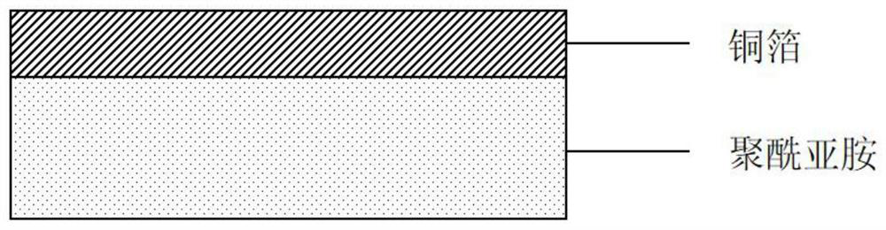
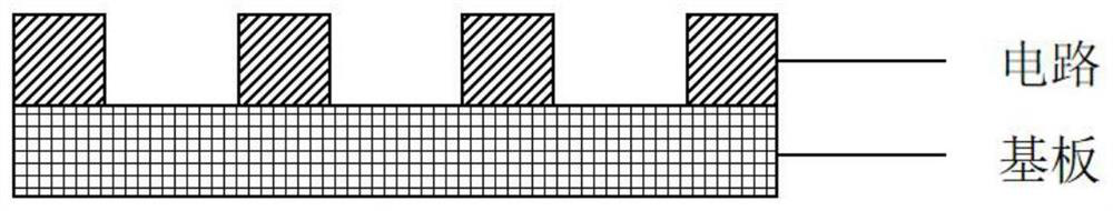
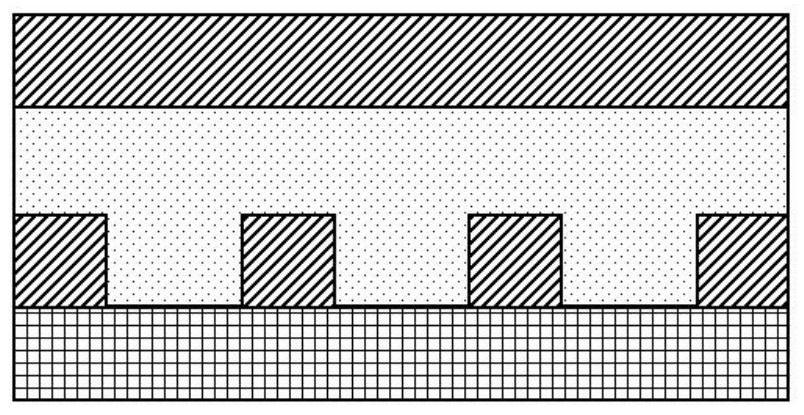
[0020] (1) Paste 20 μm copper foil on 80 μm polyimide film to obtain copper foil / polyimide two-layer film (obtained plane diagram is attached figure 1 shown), and then place the copper foil / polyimide two-layer film on top of the circuit board (the planing diagram of the circuit board is shown in the attached figure 2 shown), put it into a hot press, raise the temperature from room temperature to 240 °C at a rate of 5 °C / min, and keep it at this temperature for 1 h under a pressure of 0.5 MPa, and then cool it to room temperature in a water cooling system, where the circuit The thickness of the circuit in the substrate is 20 μm, and the thickness of the substrate is 20 μm. The planing diagram of the obtained laminate is shown in the attached image 3 shown;
[0021] (2) use 2wt% ferric chloride aqueous solution at room temperature and 2Kgf / cm 2 The copper foil on the product obtained in step (1) is etched for 1 min under the spray pressure to form an opening on the copper fo...
Embodiment 2
[0026] (1) Paste 20μm copper foil on 80μm polyimide film to obtain copper foil / polyimide two-layer film, then place copper foil / polyimide two-layer film on top of the circuit board and put it into a hot press In the process, the temperature is raised from room temperature to 240°C at a rate of 5°C / min, and kept at this temperature for 1h under a pressure of 0.5MPa, and then cooled to room temperature in a water cooling system, wherein the thickness of the circuit in the circuit substrate is 20μm, and the substrate Thickness 20μm;
[0027] (2) use 2wt% ferric chloride aqueous solution at room temperature and 2Kgf / cm 2 The copper foil on the product obtained in step (1) is etched for 2min under a spray pressure of 100%, forming an opening on the copper foil, wherein the diameter of the opening is 40 μm;
[0028] (3) consistent with the process of step (3) in embodiment 1;
[0029] (4) consistent with the process of step (4) in embodiment 1;
[0030] (5) consistent with the pr...
Embodiment 3
[0032](1) Paste 20μm copper foil on 40μm polyimide film to obtain copper foil / polyimide two-layer film, then place copper foil / polyimide two-layer film on top of the circuit board and put it into a hot press In the process, the temperature is raised from room temperature to 240°C at a rate of 5°C / min, and kept at this temperature for 1h under a pressure of 0.5MPa, and then cooled to room temperature in a water cooling system, wherein the thickness of the circuit in the circuit substrate is 20μm, and the substrate Thickness 20μm;
[0033] (2) consistent with the process of step (2) in embodiment 1;
[0034] (3) Using the above etched copper foil pattern as a mask, process the polyimide film with a carbon dioxide laser beam to form blind holes, wherein the carbon dioxide laser beam is a pulsed laser, the laser pulse width is 5 μs, and the output energy is 20W , the laser energy per pulse is 48.8mJ, and the energy density is 95J / cm 2 After each irradiating 5 pulses, blow 20L / mi...
PUM
| Property | Measurement | Unit |
|---|---|---|
| thickness | aaaaa | aaaaa |
| thickness | aaaaa | aaaaa |
| thickness | aaaaa | aaaaa |
Abstract
Description
Claims
Application Information
 - R&D
- Intellectual Property
- Life Sciences
- Materials
- Tech Scout
- Unparalleled Data Quality
- Higher Quality Content
- 60% Fewer Hallucinations
Browse by: Latest US Patents, China's latest patents, Technical Efficacy Thesaurus, Application Domain, Technology Topic, Popular Technical Reports.
© 2025 PatSnap. All rights reserved.Legal|Privacy policy|Modern Slavery Act Transparency Statement|Sitemap|About US| Contact US: help@patsnap.com