

Film electrode, preparation method and application thereof
A thin-film electrode and electrode layer technology, which is applied in cable/conductor manufacturing, equipment for manufacturing conductive/semiconductive layers, circuits, etc., can solve problems such as expensive equipment, poor shadow elimination effect, and low product yield, and achieve High production efficiency, high yield, good anti-aging effect
- Summary
- Abstract
- Description
- Claims
- Application Information
AI Technical Summary
Problems solved by technology
Method used
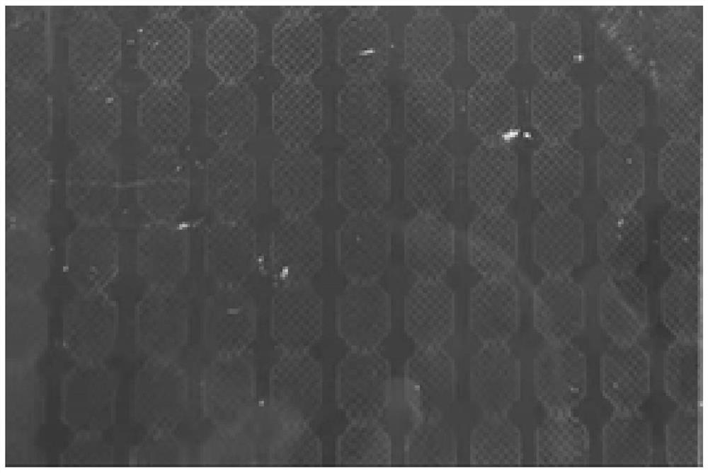
Image

Examples
Embodiment 1
[0049] Hydrolyze ethyl orthosilicate in ethanol to obtain silica sol. Divide the silica sol into two parts, of which the silica sol I is used to prepare insulating glue, and the silica sol II is used to dope metal ions.
[0050] S1 Dissolve polyimide in ethanol, add the silica sol I and dry at 50°C to obtain nano-insulation glue; wherein, the mass ratio of silica sol I and polyimide is 1:200. The nano metal silver wire is mixed with the nano insulating glue in butanol to obtain the nano metal wire ink. The mass ratio of nanometer metal silver wire, butanol and insulating glue is 1:100:5.
[0051] S2 Hydrolyze ethyl orthosilicate in water to obtain silica sol II, then add sodium chloride to silica sol II, and age at 180°C for 8 hours to obtain conductive ink; among them, ethyl orthosilicate, water, chloride The mass ratio of sodium and butanol is 1:5:1:200.
[0052] S3 laying the nano metal wire ink on the surface of the base layer by spraying;
[0053] S4 screen printing t...
Embodiment 2
[0057] Hydrolyze ethyl orthosilicate in ethanol to obtain silica sol. Divide the silica sol into two parts, of which the silica sol I is used to prepare insulating glue, and the silica sol II is used to dope metal ions.
[0058] S1 Dissolve polybenzoxazine in ethanol, add the silica sol I and dry at 50°C to obtain nano-insulation glue; wherein, the mass ratio of silica sol I to polyimide is 1:250. The nano metal gold wire and the nano insulating glue are mixed in butanol to obtain the nano metal wire ink. The mass ratio of nanometer metal silver wire, butanol and insulating glue is 1:150:8.
[0059] S2 Hydrolyze ethyl orthosilicate in water to obtain silica sol II, then add aluminum chloride to silica sol II, and age at 180°C for 12 hours to obtain conductive ink; among them, ethyl orthosilicate, water, chloride The mass ratio of aluminum and butanol is 1:20:5:400.
[0060] S3 laying the nano metal wire ink on the surface of the base layer by spraying;
[0061] S4 screen p...
Embodiment 3
[0065] Hydrolyze ethyl orthosilicate in ethanol to obtain silica sol. Divide the silica sol into two parts, of which the silica sol I is used to prepare insulating glue, and the silica sol II is used to dope metal ions.
[0066] S1 Dissolve polysiloxane in ethanol, add the silica sol I and dry at 50°C to obtain nano-insulation glue; wherein, the mass ratio of silica sol I to polyimide is 1:300. The nano metal copper wire and the nano insulating glue are mixed in butanol to obtain the nano metal wire ink. The mass ratio of nanometer metal silver wire, butanol and insulating glue is 1:200:20.
[0067] S2 Hydrolyze ethyl orthosilicate in water to obtain silica sol II, then dope copper chloride into silica sol II, and age at 180°C for 20 hours to obtain conductive ink; among them, ethyl orthosilicate, water, chloride The mass ratio of copper and butanol is 1:5:1:200.
[0068] S3 laying the nano metal wire ink on the surface of the base layer by spraying;
[0069] S4 screen pri...
PUM
 Abstract
Description
Claims
Application Information