Wafer pattern etching method, film resonator assembly and preparation method

A wafer and pattern technology, used in semiconductor/solid-state device manufacturing, electrical components, impedance networks, etc., can solve problems such as difficult sealing, depression, 20 cracks in silicon microcap wafers, etc., to improve yield, improve The degree of sealing and the effect of avoiding stress concentration

Pending Publication Date: 2021-12-17
SUZHOU HUNTERSUN ELECTRONICS CO LTD
View PDF0 Cites 0 Cited by
  • Summary
  • Abstract
  • Description
  • Claims
  • Application Information

AI Technical Summary

Problems solved by technology

However, since the edge-off region 20b is not covered by the photoresist 30, during the formation of the etching pattern 21 of the silicon micro-cap wafer 20, the silicon micro-cap wafer 20 in the edge-off region 20b will also be etched, and then As a result, a recessed structure 22 appears in the edge-cut region 20b of the silicon micro-capped wafer 20
The above-mentioned technical scheme, in the first aspect, the recessed structure 22 existing in the silicon micro-cap wafer 20 will cause the device wafer 10 and the silicon micro-cap wafer 20 to be in the bonding process, and the device wafer 10 and the silicon micro-cap wafer 20 It is difficult to

Method used


Image

  • Wafer pattern etching method, film resonator assembly and preparation method
  • Wafer pattern etching method, film resonator assembly and preparation method
  • Wafer pattern etching method, film resonator assembly and preparation method

Examples


Embodiment Construction

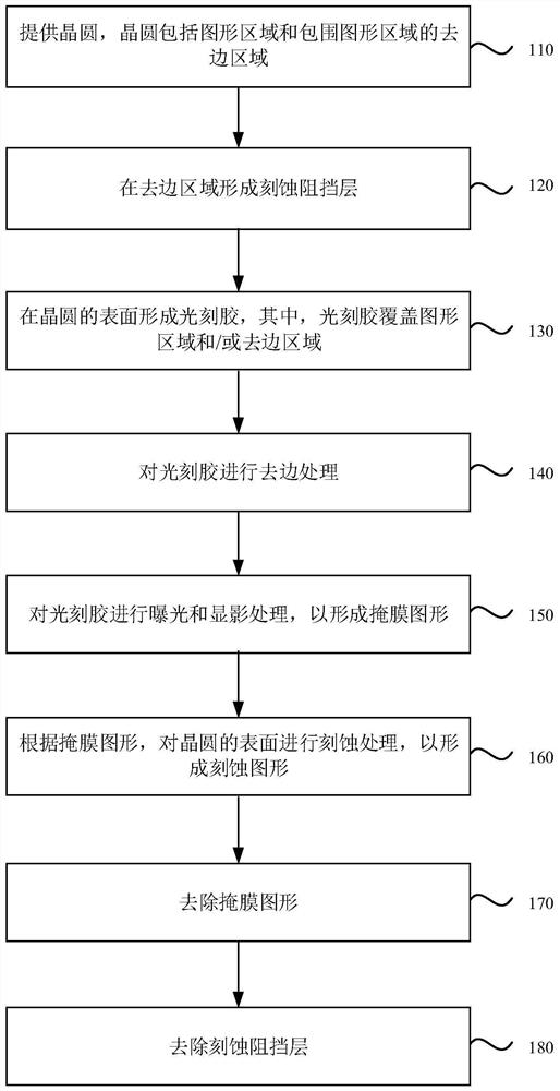
[0045] The present invention will be further described in detail below in conjunction with the accompanying drawings and embodiments. It should be understood that the specific embodiments described here are only used to explain the present invention, but not to limit the present invention. In addition, it should be noted that, for the convenience of description, only some structures related to the present invention are shown in the drawings but not all structures.

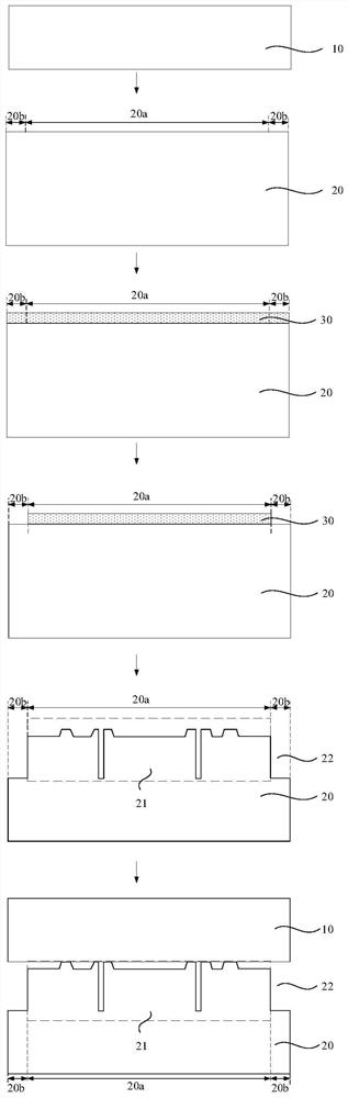
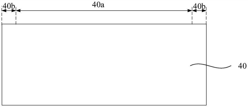
[0046] In the embodiment of the present invention, see Figure 14 and Figure 15 The thin film resonator assembly shown, the thin film resonator assembly includes: a device wafer 70, at least one resonant unit is arranged on the device wafer 70; a silicon micro-cap wafer 40, wherein the silicon micro-cap wafer 40 includes a pattern area 40a, the edge-removing area 40b surrounding the graphic area 40a. The pattern area 40a includes an etching pattern 41; the edge-removing area 40b is provided with a bonding layer...


PUM


Abstract

The embodiment of the invention discloses a wafer pattern etching method, a film resonator assembly and a preparation method. The wafer pattern etching method comprises the following steps: providing a wafer, wherein the wafer comprises a pattern area and an edge removing area surrounding the pattern area; forming an etching barrier layer in the edge removing area, wherein the etching selection ratio of the wafer to the etching barrier layer is larger than or equal to a preset etching selection ratio; forming a photoresist on the surface of the wafer, wherein the photoresist covers the pattern area and/or the edge removing area; carrying out edge removal treatment on the photoresist; performing exposure and development treatment on the photoresist to form a mask pattern; etching the surface of the wafer according to the mask pattern to form an etched pattern; removing the mask pattern; and removing the etching barrier layer. According to the technical scheme provided by the embodiment of the invention, the silicon micro cover wafer which is free of a sunken structure, simple in preparation process and low in preparation cost and the film resonator assembly which is good in sealing performance and high in yield are realized.

Description

technical field [0001] Embodiments of the present invention relate to the field of semiconductor technology, and in particular to a pattern etching method of a wafer, a thin film resonator component and a preparation method. Background technique [0002] With the continuous development of wireless communication technology, Film Bulk Acoustic Resonator (Film Bulk Acoustic Resonator) is also called Bulk Acoustic Wave, because of its small size, high operating frequency, low power consumption, high quality factor, Compatible with CMOS technology and other characteristics, it has become an important device in the field of radio frequency communication and is widely used. [0003] figure 1 It is a schematic cross-sectional structure diagram corresponding to each step of a method for preparing a thin film resonator component in the prior art. see figure 1 , the thin film resonator assembly includes a device wafer 10 and a silicon microcap wafer 20 fixedly connected by a bonding...

Claims


Application Information

Patent Timeline
IPC IPC(8): H01L21/027H03H3/02H03H9/02H03H9/56H03H9/58H03H9/70
CPCH01L21/0273H01L21/0274H03H3/02H03H9/02007H03H9/582H03H9/564H03H9/706H03H2003/023
Inventor 钱盈杨清华
Owner SUZHOU HUNTERSUN ELECTRONICS CO LTD
Why Eureka
Try Eureka