Semiconductor integrated circuit and memory

An integrated circuit and semiconductor technology, applied in static memory, digital memory information, information storage, etc., can solve problems such as the need to improve read and write performance, and achieve the effects of improving electrical performance, reducing quantity, and reducing power consumption

Pending Publication Date: 2021-12-21
CHANGXIN MEMORY TECH (SHANGHAI) INC
View PDF0 Cites 5 Cited by
  • Summary
  • Abstract
  • Description
  • Claims
  • Application Information

AI Technical Summary

Problems solved by technology

[0004] However, the read and write performance of current DRAM still needs to be improved.

Method used


Image

  • Semiconductor integrated circuit and memory
  • Semiconductor integrated circuit and memory
  • Semiconductor integrated circuit and memory

Examples


Embodiment Construction

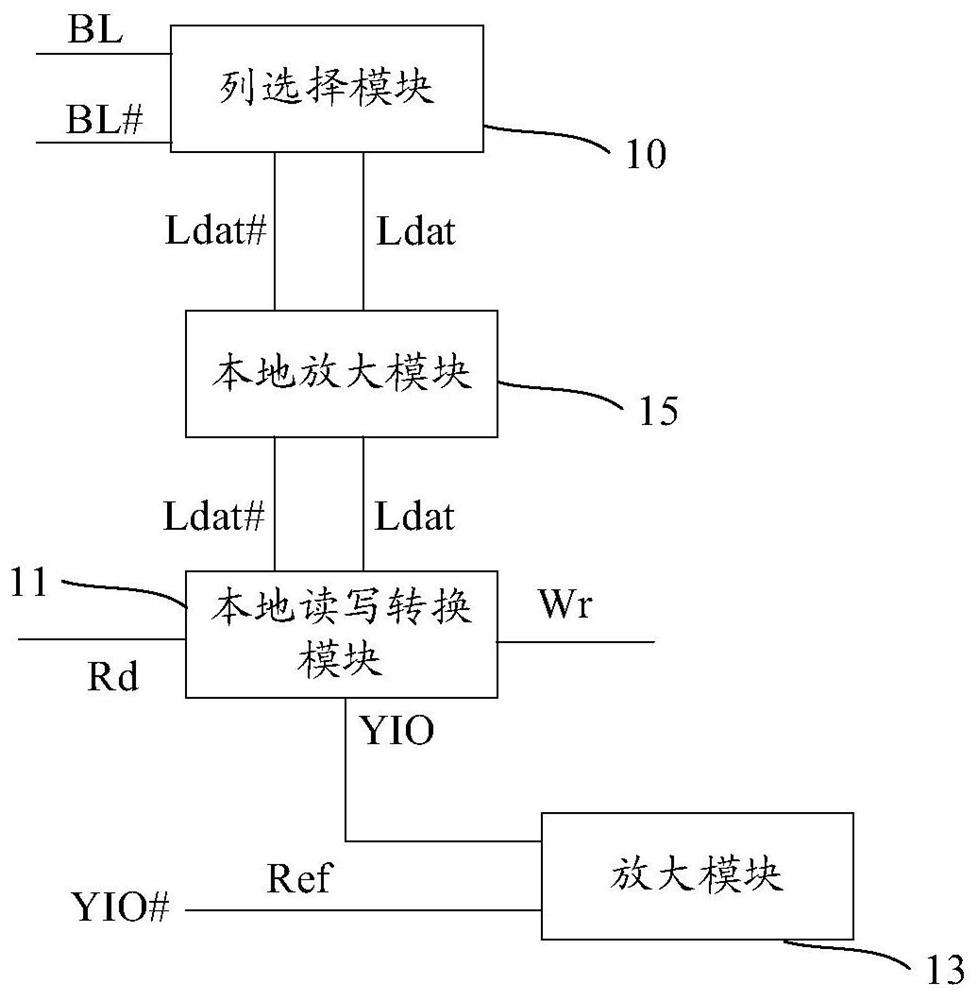
[0042] It can be seen from the background art that the current read and write performance of DRAM still needs to be improved.

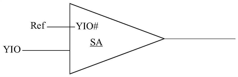
[0043] In a DRAM read operation, after the selected word line is activated, the data in the corresponding memory cell will be transferred to the bit line, causing the voltage on the bit line to slightly increase or decrease. A sense amplifier connected to the bit line, that is, a first-stage amplifier (FSA, first sense amplifier), will pull the bit line signal to 0 or 1 according to the weak signal. The column selection module transmits the 0 or 1 signal on the selected bit line to the local data line according to the column selection signal, and then transmits the signal in the local data line to the global data line through the semiconductor integrated circuit. In the DRAM write operation, the direction of signal transmission is opposite to that in the aforementioned read operation.

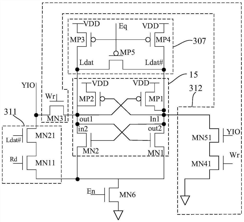
[0044] The currently commonly used signal transmission method is...


PUM


Abstract

The embodiment of the invention relates to a semiconductor integrated circuit and a memory. The semiconductor integrated circuit comprises a first data line connected with a bit line through a column selection module, and a first complementary data line, a second data line and a reference data line which are connected with a complementary bit line through the column selection module, the reference data line is used for providing a reference signal; the semiconductor integrated circuit further includes: a local read-write conversion module which responds to a read-write control signal and transmits data between the first data line and the second data line and data between the first complementary data line and the second data line during read-write operation; and an amplification module which is used for receiving the data signal of the second data line and the reference signal and amplifying the data signal of the second data line, wherein the reference signal is used as a reference for amplifying the data signal of the second data line. According to the embodiment of the invention, the electrical performance of the semiconductor integrated circuit can be improved.

Description

technical field [0001] The invention relates to the technical field of semiconductors, in particular to a semiconductor integrated circuit and a memory. Background technique [0002] Dynamic Random Access Memory (Dynamic Random Access Memory, DRAM) is a semiconductor storage device commonly used in computers, and is composed of many repeated storage units. Each memory cell usually includes a capacitor and a transistor. The gate of the transistor is connected to the word line, the drain is connected to the bit line, and the source is connected to the capacitor. The voltage signal on the word line can control the opening or closing of the transistor, and then through the bit line Read the data information stored in the capacitor, or write the data information into the capacitor through the bit line for storage. [0003] DRAM can be divided into Double Data Rate (DDR) DRAM, GDDR (Graphics Double Data Rate) DRAM, and Low Power Double Data Rate (LPDDR) DRAM. As DRAM is applied ...

Claims


Application Information

Patent Timeline
Patent Type & Authority Applications(China)
IPC IPC(8): G11C11/409G11C11/4093G06F3/06
CPCG11C11/409G11C11/4093G06F3/061G06F3/0602G06F3/06
Inventor 尚为兵陈继兴武贤君
Owner CHANGXIN MEMORY TECH (SHANGHAI) INC
Why Eureka
Try Eureka