Read-write system and method compatible with two-dimensional structure data

A two-dimensional structure, data reading and writing technology, applied in the field of data processing, can solve problems such as slowing down the actual operation of the system, processing efficiency, etc., to achieve the effect of improving hit rate, improving operation efficiency, and accelerating throughput

Active Publication Date: 2022-01-04
NANJING SEMIDRIVE TECH CO LTD
View PDF5 Cites 1 Cited by
  • Summary
  • Abstract
  • Description
  • Claims
  • Application Information

AI Technical Summary

Problems solved by technology

For data sources that exist in peripheral memory (DDR external memory, etc.) in two-dimensional form, such as digital images, sensor acquisition data, and neural network data stored in a similar form that can be equivalent to a large matrix, the algorithm logic often needs to be obtained one by one. A square area with m rows and n columns (or vector form, which can be regarded as the distortion of a matrix) of a two-dimensional data file or a two-dimensional graphic area of ​​other shapes is used for scientific operations such as convolution operations and iterative operations, while This kind of unit area with multiple consecutive calculations has a certain spatial and time domain continuity that is displaced from the center point of the area to the surroundings, so the unit area will have considerable overlap between consecutive multiple operations (such as figure 1 ), intuitively, this requires that when reading data from external memory to refresh the cache, the overlapping part should be kept in the cache as long as possible, and the unit area can be acquired by the operation processing unit faster, otherwise it will slow down the system Actual operation and processing efficiency

Method used


Image

  • Read-write system and method compatible with two-dimensional structure data
  • Read-write system and method compatible with two-dimensional structure data
  • Read-write system and method compatible with two-dimensional structure data

Examples


Embodiment 1

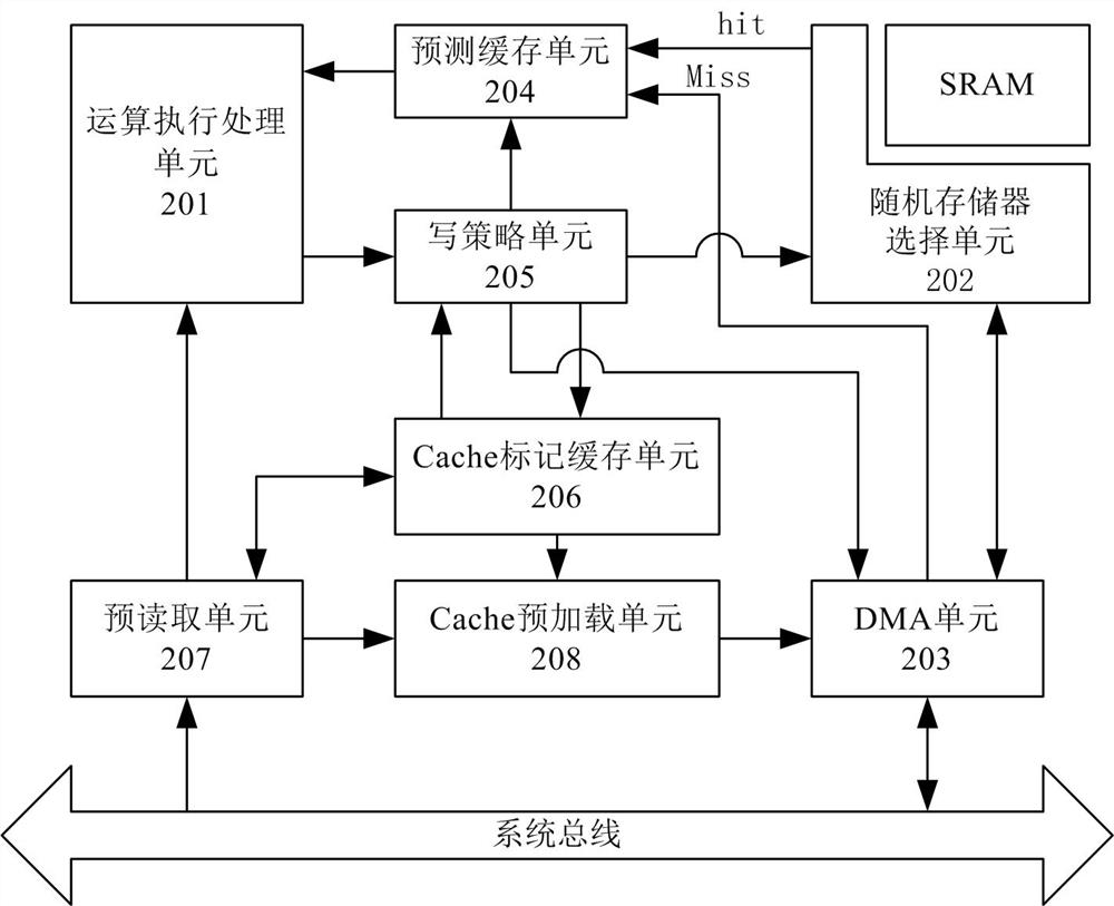
[0055] figure 2 It is a schematic diagram of a compatible two-dimensional structure data reading and writing system according to the present invention, such as figure 2 As shown, the compatible two-dimensional structured data reading and writing system of the present invention includes arithmetic execution processing unit (arithmetic execution unit) 201, random access memory selection unit (SRAM RW arbiter) 202, DMA unit 203, and prediction buffer unit (Prediction buffer) 204 , write strategy unit (write strategy) 205, Cache tag cache unit (Cache TAG buffer) 206, Cache preload unit (Cache preload) 207, and prefetch unit (prefetch) 208, wherein,

[0056] An arithmetic execution unit (arithmetic execution unit) 201 executes arithmetic instructions to read two-dimensional structure data from the predictive cache unit 204 to perform calculations, and sends the calculation results to the write strategy unit 205 .

[0057] The random memory selection unit (SRAM RW arbiter) 202 es...

Embodiment 2

[0066] Figure 4 For the flow chart of the method for reading and writing compatible two-dimensional structured data according to the present invention, reference will be made below Figure 4 , the method for reading and writing compatible two-dimensional structured data of the present invention is described in detail.

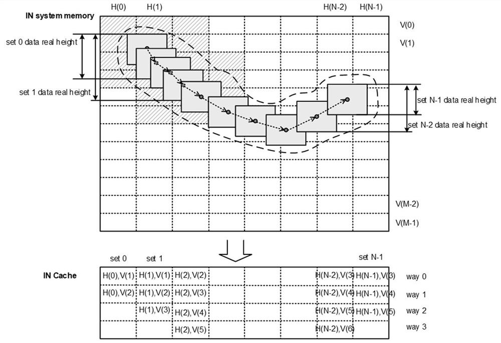
[0067] First, in step 401, the mapping structure of the Cache is determined, and the two-dimensional data is cache-mapped.

[0068] Such as figure 1 As shown, a data file in the system memory can be divided in a two-dimensional manner. Each line occupies a fixed number of bytes (bytes), which is recorded as stride, and the number of lines is recorded as lines. The dotted line is divided into squares, squares The width and height are tile_hsize and tile_vsize respectively. The physical address of the data file is file_addr, and the file size is file_size. The above parameters can be set as Cache registers. Register configurable values ​​can be as follows: ...

Embodiment 3

[0097] The present invention also provides a compatible two-dimensional structure data reading and writing chip, including the above-mentioned compatible two-dimensional structure data reading and writing system, which efficiently loads the operation data into the cache, maximizes the use of the bandwidth for accessing external memory, and improves the access of the operation unit. The hit rate of the cache speeds up the throughput of the computing unit to obtain data, thereby making full use of the computing resources in the digital logic system of the chip, and at the same time making full use of the actual physical device SRAM resources of the Cache, which is compatible with the general n-way combination mapping (n-way set-associative mapping) way. .


PUM


Abstract

A read-write system compatible with two-dimensional structure data comprises a random access memory selection unit which reads and writes an SRAM (Static Random Access Memory) according to a read-write demand of instruction decoding of an operation execution unit; a prediction caching unit which is used for performing prediction caching on two-dimensional data required by instruction execution; a writing strategy unit which is used for formulating a strategy for writing data into the SRAM and writing back an external memory; a Cache mark caching unit which is used for caching the value mark of the Cache and the state value of the square block; a Cache preloading unit which is used for generating a corresponding block refreshing request according to an updating flag bit of the Cache mark cache unit, and putting the corresponding block refreshing request into the DMA unit request queue to update the Cache; and a pre-reading unit which is used for analyzing the operation tasks according to preset batches and marking the tasks. According to the system provided by the invention, the operation efficiency of the system with the vector processing capability is greatly improved.

Description

technical field [0001] The invention relates to the technical field of data processing, in particular to a system and method for reading and writing compatible two-dimensional structure data. Background technique [0002] In the digital logic system, in order to balance the relationship between the access of the slower storage unit and the high-speed operation processing unit, it is often necessary to introduce a Cache (caching) design. For data sources that exist in peripheral memory (DDR external memory, etc.) in two-dimensional form, such as digital images, sensor acquisition data, and neural network data stored in a similar form that can be equivalent to a large matrix, the algorithm logic often needs to be obtained one by one. A square area with m rows and n columns (or vector form, which can be regarded as the distortion of a matrix) of a two-dimensional data file or a two-dimensional graphic area of ​​other shapes is used for scientific operations such as convolution ...

Claims


Application Information

Patent Timeline
Patent Type & Authority Applications(China)
IPC IPC(8): G06F12/0862G06F12/0864G06F12/0804
CPCG06F12/0862G06F12/0864G06F12/0804G06F2212/1021G06F2212/1016G06F2212/1028
Inventor 李鹏张力航
Owner NANJING SEMIDRIVE TECH CO LTD
Why Eureka
Try Eureka