Wafer-level through-silicon-via packaging structure manufacturing method and through-silicon-via packaging structure

A technology of packaging structure and manufacturing method, which is applied in semiconductor/solid-state device manufacturing, electrical components, electric solid-state devices, etc., can solve problems such as increasing costs, affecting product reliability, and stress affecting film quality, so as to reduce production costs and simplify Production process flow, effect of reduced requirements

Pending Publication Date: 2022-01-07
CHINA WAFER LEVEL CSP
View PDF0 Cites 2 Cited by
  • Summary
  • Abstract
  • Description
  • Claims
  • Application Information

AI Technical Summary

Problems solved by technology

The insulating layer and metal layer deposited here will form an outer chamfer shape, which has a great impact on product reliability
Moreover, in the process of film deposition (including metal and insulating layers) of deep holes, the coverage in the holes of the film is low. Taking the aspect ratio of 2:1 as an example, the coverage in the holes is 20% to 35%. To make the holes When the thickness of the film inside, especially at the bottom of the hole, reaches the target value, the film thickness on the surface of the hole will be greatly increased, so a large stress will affect the film quality, and will greatly increase the cost

Method used


Image

  • Wafer-level through-silicon-via packaging structure manufacturing method and through-silicon-via packaging structure
  • Wafer-level through-silicon-via packaging structure manufacturing method and through-silicon-via packaging structure
  • Wafer-level through-silicon-via packaging structure manufacturing method and through-silicon-via packaging structure

Examples


Embodiment 1

[0047] like figure 1 As shown, a method for manufacturing a 2-level through-silicon via packaging structure provided by Embodiment 1 of the present invention includes steps:

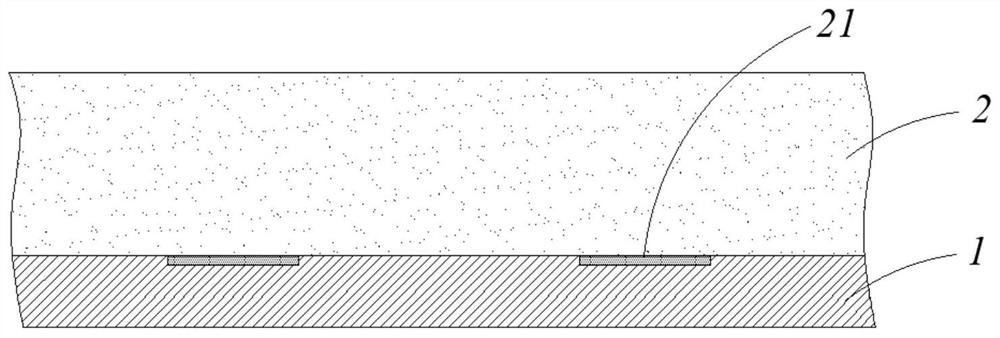
[0048] S11: If figure 2 As shown, a wafer 2 and a substrate 1 provided with bonding pads 21 are provided, and the wafer 2 is covered on the substrate 1 with the bonding pads 21 facing the direction of the substrate 1 .

[0049] The substrate 1 can be a material with a certain thickness and hardness such as bare silicon chip, glass, resin, etc., or it can be a thick adhesive tape. Different materials for the substrate 1 can be selected according to different chip functions. An adhesive layer is coated on the substrate 1 for bonding and fixing it with the wafer 2 .

[0050] A plurality of chip units arranged in an array are formed on the wafer 2, and a passivation layer is provided on one side of the wafer 2, and a plurality of welding pads 21 are distributed inside the passivation layer, serving as the...

Embodiment 2

[0070] The manufacturing method of the 2-level TSV packaging structure on the wafer in Example 2 is basically similar to that of Example 1, and the difference from Example 1 lies in:

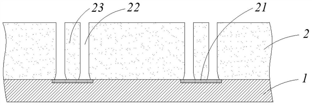
[0071] like Figure 7a As shown, in step S4, only the dry film 3a on the middle part of the upper surface of the residual silicon 23 is photolithographically exposed to expose the middle part of the residual silicon 23, and the dry film 3a on the upper surface of the outer ring of the remaining silicon 23 is not etched.

[0072] like Figure 7b As shown, a through hole 24 exposing the pad 21 is formed in the middle part of the etched residual silicon 23, and an annular silicon layer 231 is formed on the inner wall surface of the dry film 3a in the outer part of the unetched residual silicon 23. like Figure 8 As shown, after the subsequent formation of the metal layer 4, the ring-shaped silicon layer 231 is sandwiched between the insulating layer 3 and the metal layer 4, which can be used as a...

Embodiment 3

[0074] The manufacturing method of wafer 2-level through-silicon via packaging structure in Example 3 is directly etched to form a through-hole, and then directly laminates the dry film 3a and the sputtered metal layer 4, which specifically includes steps:

[0075] S21 : providing a wafer 2 and a substrate 1 provided with bonding pads 21 , and covering the wafer 2 on the substrate 1 with the bonding pads 21 facing the substrate 1 .

[0076] S22 : forming a through hole on the wafer 2 , and making at least a partial overlap between the outside of the through hole and the bonding pad 21 .

[0077] S23: Laminating a layer of dry film 3a on the surface of the wafer 2, and laminating the dry film 3a into the through hole so that it completely fills the through hole.

[0078] S24 : removing part of the insulating layer 3 located in the through hole to form a through hole 24 exposing the pad 21 .

[0079] S25 : Depositing a seed layer 41 on the surface of the insulating layer 3 and ...


PUM

PropertyMeasurementUnit
thicknessaaaaaaaaaa

Abstract

The invention provides a wafer-level through-silicon-via packaging structure manufacturing method and a through-silicon-via packaging structure. The method comprises the steps of providing a wafer provided with a welding pad and a substrate, and enabling the wafer to cover the substrate in the direction that the welding pad faces the substrate; forming an annular through hole in the wafer, and enabling the outer contour of the annular through hole and the welding pad to be at least partially overlapped; covering the surface of the wafer with an insulating layer, and filling the annular through hole with the insulating layer; forming a through hole in an area, which is located in the inner contour of the annular through hole, of the wafer, wherein the through hole exposes the welding pad; and forming a metal layer electrically connected to the welding pad on the surface of the insulating layer and in the through hole. By using the annular through hole, an inner chamfer structure is formed at the bottom of the bonding surface between the insulating layer and the metal layer, so that the requirements on the thickness and the structural uniformity of each layer in the packaging structure are greatly reduced, the production process flow is remarkably simplified without high-end equipment and process requirements by forming the insulating layer in cooperation with a dry film pressing process, and the production cost is reduced.

Description

technical field [0001] The invention relates to the field of packaging technology, in particular to a method for manufacturing a wafer-level through-silicon via packaging structure and a through-silicon via packaging structure. Background technique [0002] With the further improvement of the integration level of CMOS products, the spacing between chip pads is getting smaller and smaller, the oblique through-hole technology used in the existing WLCSP packaging through silicon vias can no longer meet the demand, and it is necessary to replace the oblique through-hole technology through-hole technology. [0003] The existing manufacturing steps of the through hole include: dry etching the straight hole, depositing an insulating layer, etching the insulating layer at the bottom of the hole to expose the welding pad, depositing metal and patterning to form a circuit layer. However, in the process steps of the above method, the etching rate of each part on the wafer will deviate...

Claims


Application Information

Patent Timeline
Patent Type & Authority Applications(China)
IPC IPC(8): H01L21/768H01L23/48
CPCH01L21/76898H01L23/481
Inventor 李瀚宇
Owner CHINA WAFER LEVEL CSP
Why Eureka
Try Eureka