Semiconductor structure and forming method thereof

A semiconductor and gate structure technology, applied in the field of semiconductor structure and its formation, can solve problems such as insufficient performance, and achieve the effects of improving production efficiency, improving performance, and improving conduction speed.

Pending Publication Date: 2022-01-07
SEMICON MFG INT (SHANGHAI) CORP +1
View PDF4 Cites 2 Cited by
  • Summary
  • Abstract
  • Description
  • Claims
  • Application Information

AI Technical Summary

Problems solved by technology

[0005] However, the gate-controlled diodes of the FinFET structure in the prior art often have the problem of insufficient performance

Method used


Image

  • Semiconductor structure and forming method thereof
  • Semiconductor structure and forming method thereof
  • Semiconductor structure and forming method thereof

Examples


Embodiment Construction

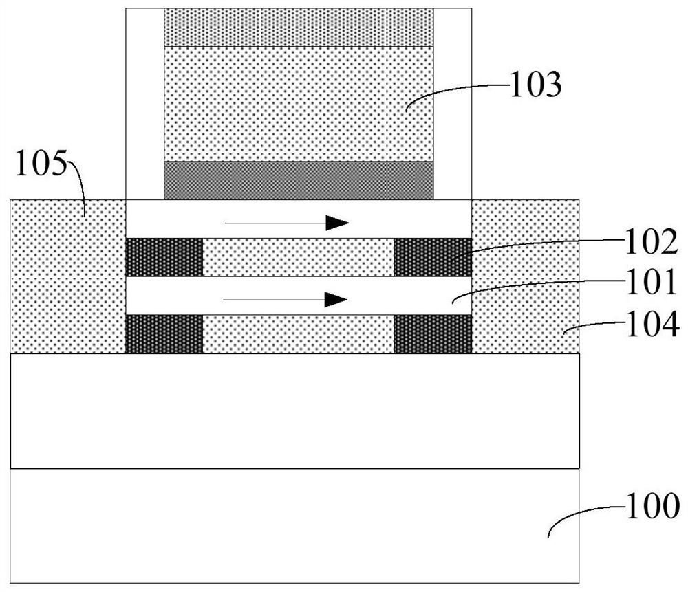
[0041] As mentioned in the background, the gate-controlled diodes of the fin field effect transistor structure in the prior art often have the problem of insufficient performance. The following will describe in detail in conjunction with the accompanying drawings.

[0042] Please refer to figure 1 , a substrate 100; a fin structure located on the substrate 100, the fin structure comprising several layers of channel layers 101 along the normal direction of the substrate surface; adjacent channel layers 101 barrier layer 102 between them; a gate structure 103 on the substrate 100, the gate structure 103 straddles the fin structure, and the gate structure 103 surrounds the channel layer 101; The first doped layer 104 and the second doped layer 105 in the fin structure, the first doped layer 104 has the first doped ions, and the second doped layer 105 has the second doped ions. hetero ions, the conductivity types of the first dopant ions and the second dopant ions are different....


PUM


Abstract

The invention relates to a semiconductor structure and a forming method thereof, and the semiconductor structure comprises a substrate which comprises diode regions arranged along a first direction; a first fin structure which is located on the diode region and comprises a plurality of first sacrificial layers and first channel layers, wherein the first sacrificial layers are overlapped in the normal direction of the surface of the substrate, and each first channel layer is located between every two adjacent first sacrificial layers; and a first gate structure which is located on the first fin structure, wherein the first gate structure stretches across the first fin structure. The first sacrificial layer is reserved in the first fin structure, so that the current of the finally formed gate-controlled diode structure can be conducted from the first sacrificial layer and the first channel layer at the same time, the conducted current of the gate-controlled diode is increased, the conduction speed is correspondingly increased, and the performance of the finally formed semiconductor structure is improved.

Description

technical field [0001] The invention relates to the technical field of semiconductor manufacturing, in particular to a semiconductor structure and a forming method thereof. Background technique [0002] With the rapid development of semiconductor manufacturing technology, semiconductor devices are developing towards higher element density and higher integration. Transistors, as the most basic semiconductor devices, are currently being widely used. Therefore, with the improvement of component density and integration of semiconductor devices, the dummy gate size of planar transistors is getting shorter and shorter. The ability of traditional planar transistors to control channel current Weakened, resulting in short channel effect, resulting in leakage current, and ultimately affecting the electrical performance of semiconductor devices. [0003] In order to overcome the short-channel effect of the transistor and suppress the leakage current, a Fin Field Effect Transistor (Fin...

Claims


Application Information

Patent Timeline
Patent Type & Authority Applications(China)
IPC IPC(8): H01L29/78H01L29/423H01L21/336
CPCH01L29/785H01L29/66803H01L29/42356
Inventor 周飞
Owner SEMICON MFG INT (SHANGHAI) CORP
Why Eureka
Try Eureka