Single-photon detector, manufacturing method thereof and single-photon detector array

A single photon detector and manufacturing method technology, applied in the direction of electric solid-state devices, semiconductor devices, final product manufacturing, etc., can solve problems such as edge breakdown, reduce the edge electric field, suppress the edge breakdown problem, and reduce complexity Effect

Active Publication Date: 2022-01-11
XIAMEN SANAN INTEGRATED CIRCUIT
View PDF11 Cites 1 Cited by
  • Summary
  • Abstract
  • Description
  • Claims
  • Application Information

AI Technical Summary

Problems solved by technology

In order to obtain a larger gain, SPAD generally works in the Geiger mode, that is, the workin

Method used


Image

  • Single-photon detector, manufacturing method thereof and single-photon detector array
  • Single-photon detector, manufacturing method thereof and single-photon detector array
  • Single-photon detector, manufacturing method thereof and single-photon detector array

Examples


Embodiment Construction

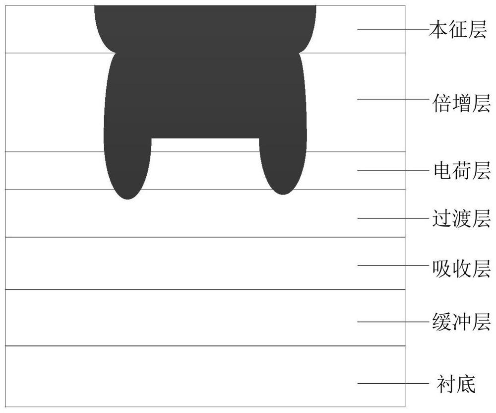
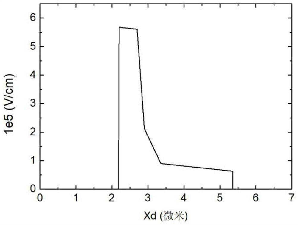
[0053] Common single photon detectors in the prior art mainly include two types. The main manufacturing process of the first method includes sequentially forming a buffer layer, an absorption layer, a transition layer, a charge layer, a multiplication layer and an intrinsic layer on a substrate. Then two diffusion processes are used to form diffusion regions in the intrinsic layer, multiplication layer and charge layer, and the formed structure is as follows figure 1 shown in . The electric field distribution diagram of the structure formed in this way is shown in figure 2 as shown in the figure 2 As shown, under the action of the charge layer, the electric field is the strongest in the multiplication layer, and the absorption layer is relatively weak, which ensures that the multiplication layer can produce collision ionization and the absorption layer does not ionize, but it can ensure that the carriers migrate at the saturation speed and increase the APD. response speed....


PUM

PropertyMeasurementUnit
Thicknessaaaaaaaaaa
Thicknessaaaaaaaaaa

Abstract

The invention provides a single-photon detector and a manufacturing method thereof, and a single-photon detector array. The method comprises the steps of sequentially growing a plurality of epitaxial layers on one side of a provided substrate, and enabling the epitaxial layers to comprise a buffer layer, an absorption layer, a transition layer, a charge layer, a multiplication layer, an inversion layer, a migration layer, a window layer, and an ohmic contact layer, and forming an arc-shaped diffusion region in the ohmic contact layer and the window layer through a diffusion process, etching the edge of a part of the epitaxial layer on the substrate to form a mesa structure, forming an optical window on the back surface of the substrate, forming a P-type electrode on the ohmic contact layer, and forming an N-type electrode on the back surface of the substrate. According to the scheme, the edge electric field of the diffusion area can be effectively reduced only through one-time diffusion treatment and combination of the inversion layer, then the edge breakdown problem is effectively restrained, and compared with an existing mode needing secondary diffusion treatment or secondary growth, the complexity of the manufacturing process is effectively reduced.

Description

technical field [0001] The invention relates to the technical field of semiconductor devices, in particular to a single photon detector, a manufacturing method thereof, and a single photon detector array. Background technique [0002] Light is composed of small energy units, that is, photons are the smallest unit of light. The energy of a single photon is about 10-19 joules in the visible light or near-infrared band, and traditional photodetectors cannot effectively detect a single photon. Single photon detectors have many advantages such as high sensitivity, high signal-to-noise ratio, and low temporal jitter. Therefore, single-photon detectors came into being. Single-photon detection technology is widely used in weak light detection fields such as quantum key distribution, laser ranging, bioluminescent detection, and DNA reaction. [0003] Currently, single photon detectors mainly include photomultiplier tubes (PMTs), superconducting single photon detectors, and single ...

Claims


Application Information

Patent Timeline
IPC IPC(8): H01L31/107H01L31/0304H01L31/18H01L27/144
CPCH01L31/107H01L31/0304H01L31/184H01L27/1443Y02P70/50
Inventor 孙维忠赵彦立陈振锋刘思远刘超邱姝颖孙久国陈文欣
Owner XIAMEN SANAN INTEGRATED CIRCUIT
Why Eureka
Try Eureka