Red copper golden PVD decorative film and preparation method thereof
A decorative thin film and golden technology, applied in metal material coating process, ion implantation plating, coating, etc., can solve the problems of uneven color deposition and low wear resistance, and achieve high color a value and wear resistance Good performance and good color uniformity
- Summary
- Abstract
- Description
- Claims
- Application Information
AI Technical Summary
Problems solved by technology
Method used
Image
Examples
preparation example Construction
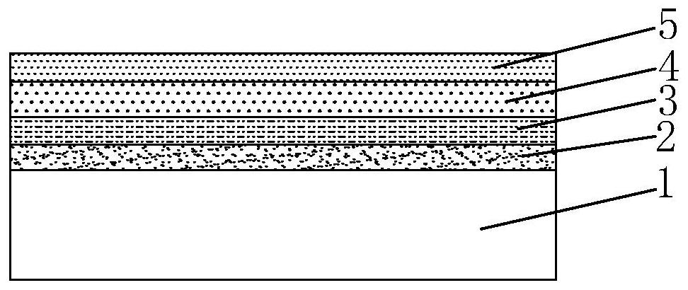
[0026] A kind of preparation method of red copper gold PVD decorative film of the present invention comprises the following steps:
[0027] Deposit a base layer on the surface of the substrate to enhance the bonding force between the film layer and the surface of the substrate;
[0028] Depositing at least one transition layer on the primer layer, the transition layer is used to enhance the bonding force between the primer layer and the color layer, and enhance the scratch resistance of the film layer;
[0029] A color layer is deposited on the transition layer (when the number of transition layers is at least two, the color layer is located on the outermost transition layer), the color a value (redness) of the color layer is 8- 11. The color b value (yellowness) is 12 to 18, which has strong reflectivity for red and yellow wavelength light, and strong absorption for blue and green wavelength light;
[0030] An interference layer is deposited on the color layer to generate li...
Embodiment 1
[0037] Multi-arc ion plating with 2 rows of 10 zirconium targets and 1 pair of intermediate frequency targets is used. After loading the samples, vacuum coating is applied. The coating process is bias glow cleaning, followed by plating of the bottom layer, transition layer, color layer, and interference layer. The coating background vacuum is 0.005pa, the coating vacuum is 0.3pa, the arc target current is 90A, and the intermediate frequency current is 30A. Other process parameters are as follows:
[0038]
[0039]
[0040] After the coating is finished, the color Lab measured by a spectrometer is: 53 / 16 / 25, and the maximum color difference ΔE of the main appearance surface of the special-shaped product is 1.9. The thickness of the color layer is 0.12 μm, and the thickness of the interference layer is 0.1 μm.
[0041]A pure interference film process is used to replace the color layer+interference layer process of the present invention to obtain similar colors, and the thi...
Embodiment 2
[0043] Multi-arc ion plating 2 rows of 10 zirconium targets, 1 pair of intermediate frequency targets, vacuum coating after loading samples. The coating process is bias glow cleaning, followed by plating the bottom layer, transition layer, color layer, and interference layer; the background vacuum of the coating is 0.005pa, the vacuum of the coating is 0.3pa, the arc target current is 90A, and the intermediate frequency current is 30A. Other process parameters are as follows:
[0044]
[0045]
[0046] After the coating is finished, the color Lab measured by a spectrometer is: 47 / 20 / 32, and the maximum color difference ΔE of the main appearance surface of the special-shaped product is 2.2. The thickness of the color layer is 0.2 μm, and the thickness of the interference layer is 0.1 μm.
[0047] A kind of preparation method of the red copper gold PVD decorative film of the present invention, the decorative film color a value that it makes is high, and color uniformity is...
PUM
| Property | Measurement | Unit |
|---|---|---|
| thickness | aaaaa | aaaaa |
| thickness | aaaaa | aaaaa |
| thickness | aaaaa | aaaaa |
Abstract
Description
Claims
Application Information


