Microelectronic packaging structure based on TSV technology

A technology of microelectronic packaging and technology, applied in circuits, electrical components, electrical solid devices, etc., can solve the problems of poor reliability, reduced yield of packaged products, warping of adapter boards, etc., to reduce volume and size. reduced effect

Pending Publication Date: 2022-01-14
TIANJIN JINHANG COMP TECH RES INST
View PDF0 Cites 0 Cited by
  • Summary
  • Abstract
  • Description
  • Claims
  • Application Information

AI Technical Summary

Problems solved by technology

[0003] However, when the interposer is used as part of the chip package, especially during the reflow process, the interposer is prone to significant warpage
During the manufacturing process of the chip package, the warpage of the interposer may cause the yield of packaged products to decrease and the reliability to deteriorate. This is the challenge faced by the field of chip packaging based on the interposer currently.

Method used


Image

  • Microelectronic packaging structure based on TSV technology
  • Microelectronic packaging structure based on TSV technology
  • Microelectronic packaging structure based on TSV technology

Examples


Embodiment 1

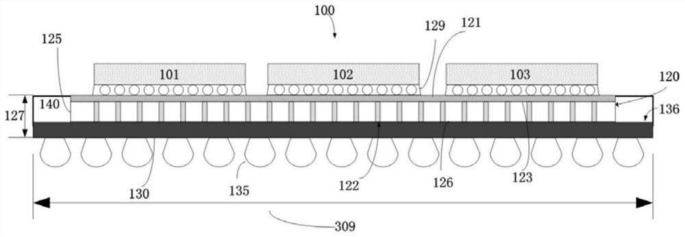
[0074] figure 1 is a schematic cross-sectional view of a microelectronic package 100 arranged in accordance with an embodiment of the present invention. Microelectronic package 100 includes IC (Integrated Circuit) chips 101 , 102 and 103 , interposer 120 , package substrate 130 and molded stiffener 140 . The microelectronic package 100 electrically and mechanically connects the components therein, including the IC chips 101, 102 and 103 and any other logic or memory IC chips mounted on the interposer board 120, and the PCB (printed circuit board) or other substrates (not shown) external to the microelectronic package 100 . In addition, microelectronic package 100 protects IC chips 101, 102, and 103 from environmental moisture and other contamination, and minimizes mechanical shock and stress thereon. For clarity, figure 2 Some components of the IC system 100 are omitted, such as some overmolding materials used to package the IC chips 101, 102 and 103, heat sinks, and the l...

Embodiment 2

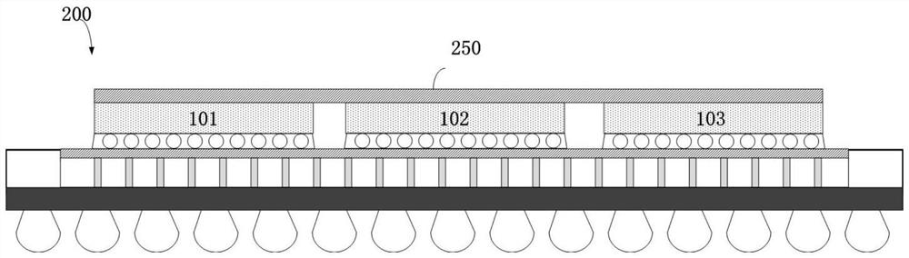
[0083] figure 2 is a schematic cross-sectional view of a microelectronic package 200 arranged in accordance with one embodiment of the invention. Microelectronic package 200 also includes heat sink 250, and microelectronic package 200 is structurally and operationally identical to figure 1 The microelectronic package 100 in is substantially similar. The heat sink 250 of the microelectronic package 200 is thermally coupled to the IC chips 101 , 102 and 103 to reduce heat generated by signal transmission between the IC chips 101 , 102 and 103 . In some embodiments, heat spreader 250 is formed from a single piece of metal with relatively high thermal conductivity, such as a stamped copper or aluminum plate. Suitable materials for making heat sink 250 include copper, aluminum, or some other metal with a thermal conductivity at least equal to that of aluminum, ie, at least about 230 Wm-1K-1.

Embodiment 3

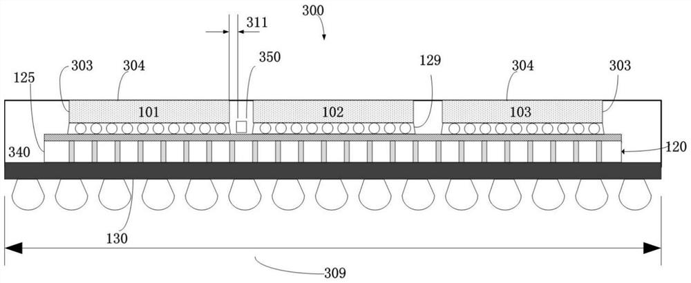
[0085] image 3 is a schematic cross-sectional view of a microelectronic package 300 arranged in accordance with one embodiment of the invention. In the microelectronic package 300, the molded stiffener 340 is configured to contact the edge surface 125 of the interposer 120, one or more surfaces of the IC chips 101, 102 and 103, and in addition the microelectronic package 300 is structurally composed and operationally with figure 1 The microelectronic package 100 in is substantially similar. In such an embodiment, a molded reinforcement plate 340 replaces the underfill material 129 . For reference, the location of underfill material 129 is at image 3 shown in . In addition, the molded stiffener 340 may also contact the edge surfaces 303 of the IC chips 101 , 102 . exist image 3 In the illustrated embodiment, molded stiffener 340 is in contact with all surfaces 303 except upper surfaces 304 of IC chips 101 , 102 and 103 .

[0086]Using molded stiffener 340 in place of ...


PUM


Abstract

The invention belongs to the technical field of integrated circuit chip packaging, and particularly relates to a microelectronic packaging structure based on a TSV technology. The structure comprises an adapter plate having through-silicon vias to which one or more semiconductor dies are coupled, wherein the semiconductor dies are connected to a first signal RDL redistribution layer on one side of the adapter plate through the through-silicon vias; a second signal RDL redistribution layer is located on the other side of the adapter plate and is electrically connected to the through-silicon vias; and a molding compound is formed on the edge surface of the adapter plate, thereby curing the microelectronic packaging structure. The microelectronic packaging structure has the advantages that the size of the microelectronic packaging structure can be obviously reduced, and the risk of warping is avoided; and the molding compound is used for replacing an underfill material to protect the electrical connection between an IC chip and the adapter plate, so that the volume size of the microelectronic package is reduced.

Description

technical field [0001] The invention belongs to the technical field of integrated circuit chip packaging, and in particular relates to a microelectronic packaging structure based on TSV technology. Background technique [0002] In the field of high-density packaging of ICs (integrated circuits), it is generally desired to achieve further miniaturization of the thickness and size of packaged chips. In today's mobile device manufacturing field, such as mobile phones, portable notebook computers, electronic tablet computers, etc., it is more urgent to minimize the IC package thickness and size of related devices, thereby further reducing the volume and weight of such mobile devices. For example, an IC package can be attached to a package substrate with an interposer that is about 100um thick, instead of a conventional package substrate that is 1mm thick or thicker. [0003] However, when the interposer is used as a part of the chip package, especially during the reflow process...

Claims


Application Information

Patent Timeline
Patent Type & Authority Applications(China)
IPC IPC(8): H01L23/31H01L23/48H01L23/29H01L25/18
CPCH01L23/3107H01L23/481H01L23/293H01L25/18H01L2924/181H01L2224/16225H01L2224/73204H01L2224/32225H01L2924/15311H01L2924/18161H01L2924/00012H01L2924/00
Inventor 朱琳朱天成张楠徐艺轩
Owner TIANJIN JINHANG COMP TECH RES INST
Why Eureka
Try Eureka