TSV back exposed hole structure and preparation method thereof
A hole structure and backside technology, applied in the field of microelectronics, can solve the problems of high cost and poor uniformity of exposed holes in the wafer, and achieve the effects of high cost, lower technical threshold and high mechanical strength.
- Summary
- Abstract
- Description
- Claims
- Application Information
AI Technical Summary
Problems solved by technology
Method used
Image

Examples
Embodiment 1
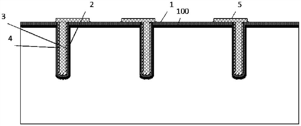
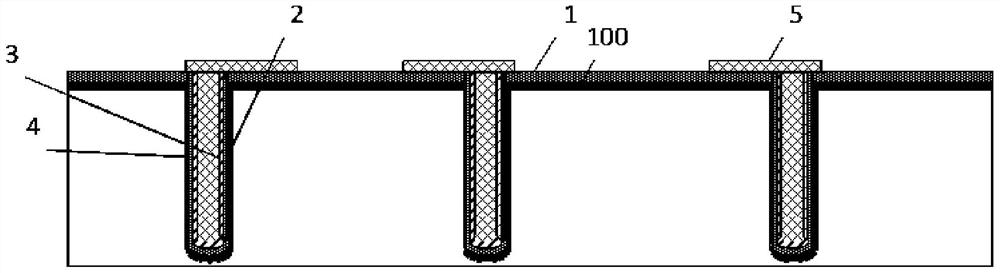
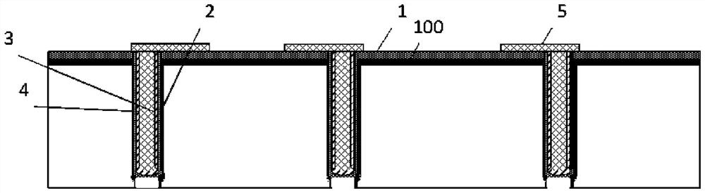
[0037] A TSV rear exposed hole structure, comprising a substrate 100, the upper surface of the substrate 100 is provided with a front insulating layer 1, and the upper surface of the substrate 100 is provided with a TSV blind hole; the front insulating layer 1 is laid with a front metal wiring layer 5 The TSV blind hole is filled with conductive filler 4, and the front metal wiring layer 5 is connected to the conductive filler 4; the lower surface of the substrate 100 is provided with a second through hole, and the second through hole is located directly below the TSV blind hole, and It is coaxial with the TSV blind hole, and the bottom of the TSV blind hole communicates with the second through hole. The lower surface of the substrate 100 is provided with a back insulating layer 6 , and a back metal wiring layer 7 is laid on the back insulating layer 6 . The back metal wiring layer 7 is located at one end of the second through hole and communicates with the second through hole....
Embodiment 2
[0039] Except for the following content, all the other contents are the same as in Example 1.
[0040] The inner wall of the TSV blind hole is provided with an insulating layer 2 in the blind hole, and an adhesive layer 3 in the blind hole is arranged between the insulating layer 2 in the blind hole and the conductive filler 4 . There are three TSV blind holes; the front metal wiring layer 5 has multiple layers, and the back metal wiring layer 7 has multiple layers. The height of the second through hole in the vertical direction is 3 μm. The diameter of the second through hole is equal to the diameter of the TSV blind hole.
Embodiment 3
[0042] Except for the following content, all the other contents are the same as in Example 1.
[0043] The height of the second through hole along the vertical direction is 6 μm; the diameter of the second through hole is larger than the diameter of the TSV blind hole.
PUM
| Property | Measurement | Unit |
|---|---|---|
| Height | aaaaa | aaaaa |
Abstract
Description
Claims
Application Information
 - R&D
- Intellectual Property
- Life Sciences
- Materials
- Tech Scout
- Unparalleled Data Quality
- Higher Quality Content
- 60% Fewer Hallucinations
Browse by: Latest US Patents, China's latest patents, Technical Efficacy Thesaurus, Application Domain, Technology Topic, Popular Technical Reports.
© 2025 PatSnap. All rights reserved.Legal|Privacy policy|Modern Slavery Act Transparency Statement|Sitemap|About US| Contact US: help@patsnap.com