Method for reducing polycrystalline silicon critical dimension loss caused by photoetching photoresist reworking

A critical dimension and polysilicon technology, applied in semiconductor/solid-state device manufacturing, electrical components, circuits, etc., can solve the problems of polysilicon critical dimension reduction, yield loss, line width loss, etc., to improve polysilicon critical dimension reduction, The effect of reducing production costs and increasing critical dimensions

Pending Publication Date: 2022-02-01
SHANGHAI HUALI MICROELECTRONICS CORP
View PDF0 Cites 0 Cited by
  • Summary
  • Abstract
  • Description
  • Claims
  • Application Information

AI Technical Summary

Problems solved by technology

[0003] However, when the Q-time overtime of polysilicon LEC etching requires photolithography and photoresist rework, it is limited by the rework process conditions, such as dry stripping, wet cleaning and other processes, which will inevitably reduce to a certain extent. Critical Dimensions of Polysilicon Hard Mask
It is easy to understand that during the rework process, the sidewalls of the oxide layer / silicon nitride layer used as a hard mask will first be bombarded by dry stripping plasma, resulting in a loss of part of the line width; after wet cleaning It will cause some loss of line width
Therefore, in the case of photolithography and photoresist rework, the final polysilicon critical dimension will become smaller after polysilicon LEC etching, the actual impact is about 1nm, and the online measurement fluctuation of about 3sigma will directly cause yield loss

Method used


Image

  • Method for reducing polycrystalline silicon critical dimension loss caused by photoetching photoresist reworking
  • Method for reducing polycrystalline silicon critical dimension loss caused by photoetching photoresist reworking
  • Method for reducing polycrystalline silicon critical dimension loss caused by photoetching photoresist reworking

Examples


Embodiment Construction

[0026] In order to illustrate the technical content, structural features, achieved goals and effects of the present invention in detail, the following will be described in detail in conjunction with the embodiments and accompanying drawings.

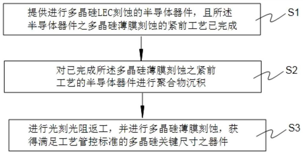
[0027] see figure 1 , figure 1 Shown is a flow chart of the method for reducing polysilicon critical dimension loss caused by photolithography and photoresist rework in the present invention. The method for reducing polysilicon critical dimension loss caused by photolithography and photoresist rework includes:

[0028] Executing step S1: providing a semiconductor device for polysilicon LEC etching, and the process immediately before the polysilicon film etching of the semiconductor device has been completed;

[0029] Executing step S2: performing polymer deposition on the semiconductor device that has completed the process immediately before the etching of the polysilicon film;

[0030] Executing step S3: performing photolithography a...


PUM

PropertyMeasurementUnit
thicknessaaaaaaaaaa
thicknessaaaaaaaaaa

Abstract

The invention discloses a method for reducing polycrystalline silicon critical dimension loss caused by photoetching photoresist reworking, which comprises the steps of S1, providing a semiconductor device for polycrystalline silicon LEC etching, wherein the just preceding process of polycrystalline silicon thin film etching is completed; S2, carrying out polymer deposition; and S3, carrying out photoetching photoresist reworking, and carrying out polycrystalline silicon thin film etching to obtain a polycrystalline silicon critical dimension device meeting the process control standard. According to the method, polymer deposition is carried out on the semiconductor device which is subjected to the just preceding process of etching the polycrystalline silicon thin film, the critical dimension of a hard mask is increased, and under the condition that the pattern of the polycrystalline silicon thin film is not changed, the problem that the critical dimension of polycrystalline silicon is reduced can be effectively solved, the product yield is improved, and the production cost is reduced.

Description

technical field [0001] The invention relates to the technical field of semiconductor manufacturing, in particular to a method for reducing the loss of critical dimensions of polysilicon caused by photolithography and photoresist rework. Background technique [0002] Driven by Moore's Law, the size of the semiconductor process is gradually shrinking, and the online control is becoming more and more stringent. At the 28nm technology node, polysilicon is etched in two steps: polysilicon hard mask etching and polysilicon LEC (LEC, Litho Edgecut) etching. In this field, as everyone knows, after the first polysilicon hard mask etching is completed, the polysilicon line width has been determined; the second polysilicon LEC etching will inherit the critical dimensions of the polysilicon hard mask (CD, CriticalDimension) etch down. [0003] However, when the Q-time overtime of polysilicon LEC etching requires photolithography and photoresist rework, it is limited by the rework proc...

Claims


Application Information

Patent Timeline
Patent Type & Authority Applications(China)
IPC IPC(8): H01L21/027H01L21/3213
CPCH01L21/0274H01L21/3213
Inventor 陈敏杰许进唐在峰任昱
Owner SHANGHAI HUALI MICROELECTRONICS CORP
Why Eureka
Try Eureka