

Sapphire substrate manufacturing method
A technology of a sapphire substrate and a manufacturing method, which is applied in the directions of electrical components, circuits, semiconductor devices, etc., can solve the problem of high cost of single-chip production
- Summary
- Abstract
- Description
- Claims
- Application Information
AI Technical Summary
Problems solved by technology
Method used
Image

Examples
Embodiment 1
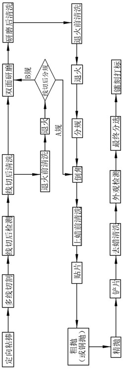
[0089] The sapphire substrate manufacturing method among the present embodiment comprises the following steps:
[0090] Obtain the wafer that has been cleaned after wire cutting, and clean the wafer that has been cleaned after wire cutting at a temperature of 130°C before annealing. The cleaning time is 10 minutes, and then anneal the wafer at a temperature of 1600°C. The time is 720 min; according to the wafer specification data, the wafer after the annealing treatment is subjected to wire-cutting and subdivision processing, and the subdivision-processed wafers are screened to obtain the screened wafers. The yield rate of the screened wafers is 100 %, the screened wafers include wafers of the first specification, and the wafer specification data of the wafers of the first specification are: Bow=-3.42 μm, Warp=12.5 μm, thickness=712.5 μm, TTV=7.5 μm; for the first specification The standard wafer is chamfered, and the sapphire substrate is obtained through the chamfered wafer....
PUM
 Abstract
Description
Claims
Application Information