MOS type power device

A technology of power devices and ceramics, applied in the field of MOS type power devices, can solve the problems of high working temperature of field effect transistors, poor heat dissipation effect, softening of solder joints, etc., and achieve the effect of facilitating heat diffusion, reducing volume and reducing thermal resistance.

Pending Publication Date: 2022-02-22
苏州秦绿电子科技有限公司
View PDF0 Cites 0 Cited by
  • Summary
  • Abstract
  • Description
  • Claims
  • Application Information

AI Technical Summary

Problems solved by technology

With the field effect tube package structure of the above structure, due to the high working temperature of the field effect tube and the poor heat dissipation effect, it is easy to cause the solder joints to soften due to high temperature

Method used


Image

  • MOS type power device
  • MOS type power device
  • MOS type power device

Examples


Embodiment 1

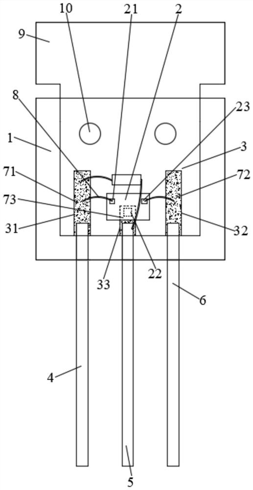
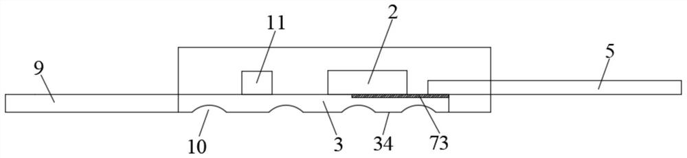
[0026] Embodiment 1: A MOS type power device, including: a MOSFET chip 2 located in an epoxy package 1, a fast recovery diode 11, a ceramic heat conducting body 3, a source pin 4, a drain pin 5 and a gate tube Pin 6, the source pin 4, the drain pin 5 and the gate pin 6 extend outward from the epoxy package 1;

[0027] One surface of the ceramic heat conducting body 3 is provided with a first strip-shaped groove 31, a second strip-shaped groove 32 and a third groove 33, and the first strip-shaped groove 31, the second strip-shaped groove 32 and the first strip-shaped groove 32 The three grooves 33 are respectively filled with a first conductive strip 71, a second conductive strip 72 and a conductive block 73;

[0028] The MOSFET chip 2 has a source region 21, a drain region 22 and a gate region 23, and the MOSFET chip 2 is mounted on a ceramic heat-conducting body, and the source region 21, the drain region 22 and the gate region 23 are respectively Electrically connected with...

Embodiment 2

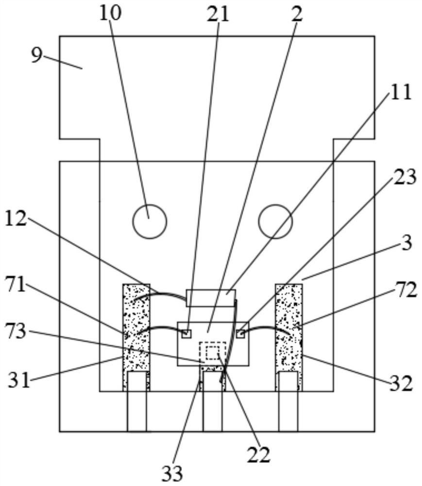
[0035] Embodiment 2: A MOS type power device, including: a MOSFET chip 2 located in an epoxy package 1, a fast recovery diode 11, a ceramic heat-conducting body 3, a source pin 4, a drain pin 5 and a gate tube Pin 6, the source pin 4, the drain pin 5 and the gate pin 6 extend outward from the epoxy package 1;

[0036] One surface of the ceramic heat conducting body 3 is provided with a first strip-shaped groove 31, a second strip-shaped groove 32 and a third groove 33, and the first strip-shaped groove 31, the second strip-shaped groove 32 and the first strip-shaped groove 32 The three grooves 33 are respectively filled with a first conductive strip 71, a second conductive strip 72 and a conductive block 73;

[0037]The MOSFET chip 2 has a source region 21, a drain region 22 and a gate region 23, and the MOSFET chip 2 is mounted on a ceramic heat-conducting body, and the source region 21, the drain region 22 and the gate region 23 are respectively Electrically connected with ...


PUM


Abstract

The invention discloses an MOS (Metal Oxide Semiconductor) type power device, which comprises an MOSFET (Metal Oxide Semiconductor Field Effect Transistor) chip, a fast recovery diode, a ceramic heat conduction body, a source electrode pin, a drain electrode pin and a grid electrode pin which are positioned in an epoxy packaging body. The source electrode pin, the drain electrode pin and the grid electrode pin extend outwards from the inside of the epoxy packaging body. The source electrode pin is electrically connected with a first conductive strip, the drain electrode pin is electrically connected with the other end of a conductive block, and the grid electrode pin is electrically connected with a second conductive strip. The ceramic heat conduction body is provided with a heat dissipation plate extending out of the end face of the epoxy packaging body, and the portion, located in the epoxy packaging body, of the ceramic heat conduction body is provided with at least one through hole. The positive electrode and the negative electrode of the fast recovery diode are connected to the first conductive strip and the conductive block through conductive gold wires. The side surface, opposite to the MOSFET chip, of the ceramic heat conduction body extends out of the epoxy packaging body. The power of the device is further improved, heat diffusion is facilitated, water vapor is prevented from entering the device, heat diffusion is facilitated, and the overall structural stability of the device is improved.

Description

technical field [0001] The invention relates to the technical field of semiconductor devices, in particular to a MOS type power device. Background technique [0002] A metal-oxide semiconductor field effect transistor, referred to as a metal oxide semiconductor field effect transistor, is a field effect transistor that can be widely used in analog circuits and digital circuits. According to the polarity of its "channel", MOSFET can be divided into two types: "N-type" and "P-type". [0003] Field effect tubes are widely used in the industrial fields of synchronous rectification switching power supply and pulse power supply. For this reason, many packaging structures of field effect tubes are involved in the prior art. Generally, the package structure of high current is to directly weld the field effect tubes on the circuit board. Then fix the circuit board on the corresponding conductive base, and finally carry out the corresponding packaging. With the field effect tube pac...

Claims


Application Information

Patent Timeline
Patent Type & Authority Applications(China)
IPC IPC(8): H01L25/18H01L23/367H01L23/373H01L23/467
CPCH01L25/18H01L23/367H01L23/3731H01L23/467H01L23/3677
Inventor 张开航马云洋
Owner 苏州秦绿电子科技有限公司
Why Eureka
Try Eureka