Method for preparing micro-nano structure on surface of base material, base material with micro-nano structure on surface and application of base material

A technology of micro-nano structure and substrate surface, which is applied in the field of material surface processing, can solve the problems of complicated process and poor shape controllability, and achieve the effect of simple operation, saving production cost, and controllable micro-nano structure shape

Pending Publication Date: 2022-03-01
WEIDALI IND CHIBI CO LTD
View PDF3 Cites 2 Cited by
  • Summary
  • Abstract
  • Description
  • Claims
  • Application Information

AI Technical Summary

Problems solved by technology

[0004] Later, it was discovered that the morphology of micro-nano structures can also be used in other fields, such as inorganic cover plates (glass cover plates, quartz, etc.) or organic material cover plates, etc. There are problems such as complex process and poor shape controllability

Method used


Image

  • Method for preparing micro-nano structure on surface of base material, base material with micro-nano structure on surface and application of base material
  • Method for preparing micro-nano structure on surface of base material, base material with micro-nano structure on surface and application of base material
  • Method for preparing micro-nano structure on surface of base material, base material with micro-nano structure on surface and application of base material

Examples


Embodiment 1

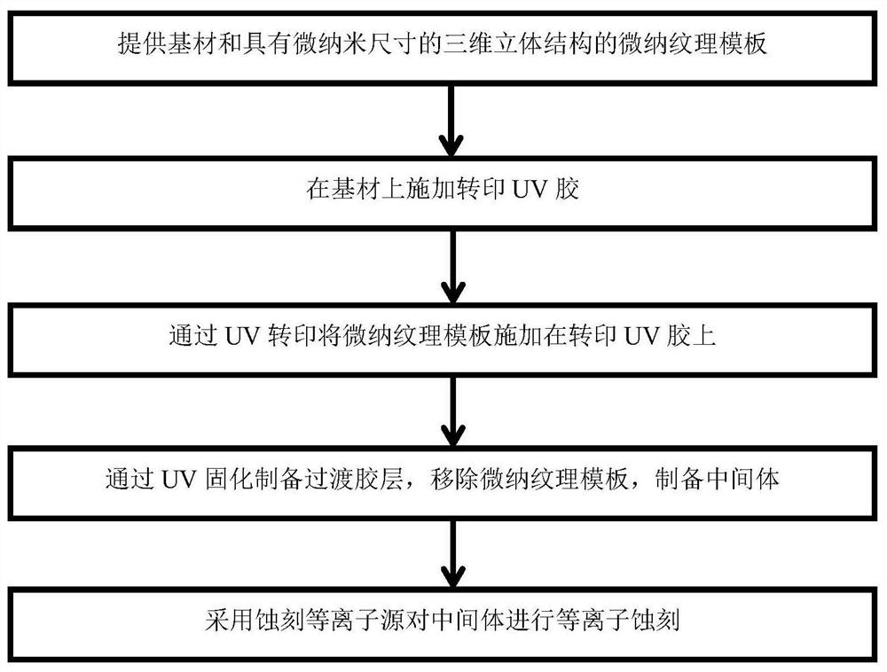
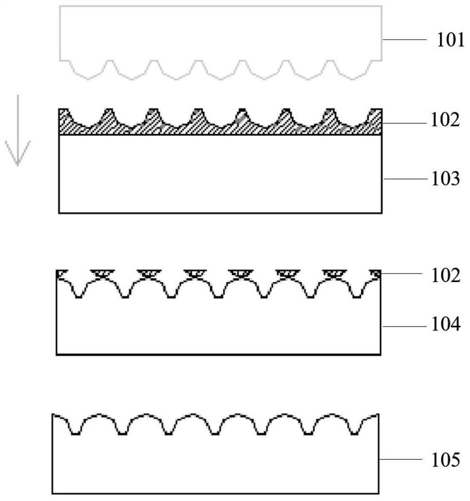
[0080] A PET film with a three-dimensional concave columnar array micro-nano texture template with a diameter of 2.5 μm and a depth of 300 nm is used as a transfer mold. The texture surface has an anti-sticking effect and does not adhere to the cured transfer UV glue.

[0081] Point the transfer UV glue line on the edge of the outer surface of the PMMA\PC composite board substrate, and then place the PET film of the transfer mold on the glue line substrate, the mold texture side faces the transfer UV glue, and the mold texture area Corresponds to the area where the substrate needs to be textured. Apply roller pressure on the outer surface of the transfer mold, and roll from one side of the dispensing line to the corresponding side, so that the transfer UV glue is completely filled between the texture surface of the transfer mold and the surface of the substrate.

[0082] Use a full-band UV surface light source with an energy of 360mJ to irradiate and transfer the UV adhesive l...

Embodiment 2

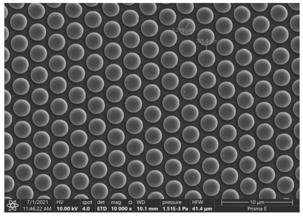
[0087] A PET film with a three-dimensional convex columnar array micro-nano texture template with a diameter of 600nm and a depth of 200nm is used as a transfer mold. The texture surface has an anti-adhesive effect and does not adhere to the cured transfer UV glue.

[0088] Point transfer UV glue line on the edge side of the outer surface of the high-alumina silica glass substrate, and then place the transfer mold PET film on the glue line substrate, the mold texture side faces the transfer UV glue, the mold texture area and The base material needs to be made corresponding to the texture area. Apply roller pressure on the outer surface of the transfer mold, and roll from one side of the dispensing line to the corresponding side, so that the transfer UV glue is completely filled between the texture surface of the transfer mold and the surface of the substrate.

[0089] Using a full-band UV surface light source with an energy of 360mJ, irradiate the UV adhesive layer for 6s, cur...

Embodiment 3

[0095] A template with surface topography of 10 μm, irregular arrangement of 1 micron depth, and dot-like topography of different sizes is used as a micro-nano texture mold. The texture surface has an anti-sticking effect and does not adhere to the cured transfer UV glue. .

[0096] On the edge of the surface of the micro-nano texture on the surface of the glass substrate, point transfer UV glue line, and then place the transfer micro-nano texture mold on the glue line substrate, the mold texture side faces the transfer UV glue, and the mold texture area Corresponds to the area where the substrate needs to be textured. Apply roller pressure on the outer surface of the transfer mold, and roll from one side of the dispensing line to the corresponding side, so that the transfer UV glue is completely filled between the texture surface of the transfer mold and the surface of the substrate.

[0097] Using a full-band UV surface light source with an energy of 800mJ, irradiate the UV...


PUM

PropertyMeasurementUnit
etching depthaaaaaaaaaa
diameteraaaaaaaaaa
diameteraaaaaaaaaa

Abstract

The invention relates to a method for preparing a micro-nano structure on the surface of a base material, the base material with the micro-nano structure on the surface and application of the base material. Comprising the following steps: providing a base material and a micro-nano texture template with a micro-nano size and a three-dimensional structure; transfer printing UV glue is applied to the base material; the micro-nano texture template is applied to the transfer printing UV glue through UV transfer printing, then a transition glue layer is prepared through UV curing, the micro-nano texture template is removed, and an intermediate is prepared; and carrying out plasma etching on the intermediate by adopting an etching plasma source so as to remove the transition glue layer in a region to be etched on the surface of the base material, and etching a three-dimensional structure with a micro-nano size on the surface of the base material. The method has the advantages of being easy to operate, controllable in micro-nano structure morphology, low in cost, long-acting and capable of being applied on a large scale. In addition, the use of exposure and development can be reduced, and the equipment cost and the manufacturing cost are saved.

Description

technical field [0001] The invention relates to the technical field of material surface processing, in particular to a method for preparing a micro-nano structure on the surface of a substrate, a substrate with a micro-nano structure on the surface and an application thereof. Background technique [0002] UV transfer printing process is also called UV infusion process or UV coating process. It uses the non-stick properties of UV transfer glue and metal to transfer the effect of various ultra-thin buttons to polyethylene terephthalate through UV transfer process. polyester (PET), polycarbonate (PC) or polymethyl methacrylate (PMMA) sheets to make, including CD pattern, brushed pattern, sun pattern, batch pattern, woven pattern, sandblasting pattern, leather Texture, 3D surface, illusion effect, bulge effect, cat's eye effect, matte surface, bright surface, high-gloss surface and other effects ultra-thin buttons, product features: (1) has good optical properties, high hardness...

Claims


Application Information

Patent Timeline
Patent Type & Authority Applications(China)
IPC IPC(8): B05D5/00B05D5/08B05D3/06B05D3/14
CPCB05D5/00B05D5/08B05D3/145B05D3/067
Inventor 李可峰
Owner WEIDALI IND CHIBI CO LTD
Why Eureka
Try Eureka