

Preparation method of semiconductor device
A semiconductor and device technology, applied in the field of semiconductor device preparation, can solve problems such as increased junction leakage current
Pending Publication Date: 2022-03-01
CHANGXIN MEMORY TECH INC
View PDF6 Cites 0 Cited by
- Summary
- Abstract
- Description
- Claims
- Application Information
AI Technical Summary
Problems solved by technology
[0004] Based on this, it is necessary to provide a semiconductor device for the problem that the distance between the metal silicide and the edge of the drain region gradually decreases and the junction leakage current gradually increases with the continuous improvement of the integration of semiconductor devices in the prior art. preparation method
Method used
View moreImage
Smart ImageViewing Examples

Examples
preparation example Construction
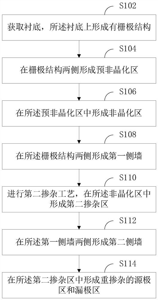
[0058] Such as figure 1 As shown, in one of the embodiments, a method for preparing a semiconductor device is provided, including:
[0059] S102, acquiring a substrate, on which a gate structure is formed.
[0060] The substrate may be a silicon substrate, a silicon-on-insulator substrate (SOI), a stacked silicon-on-insulator substrate (SSOI), a stacked silicon-germanium-on-insulator substrate (S-SiGeOI), or a silicon-germanium-on-insulator substrate (SiGeOI) and germanium-on-insulator substrate (GeOI) and so on.
Login to View More PUM
 Abstract
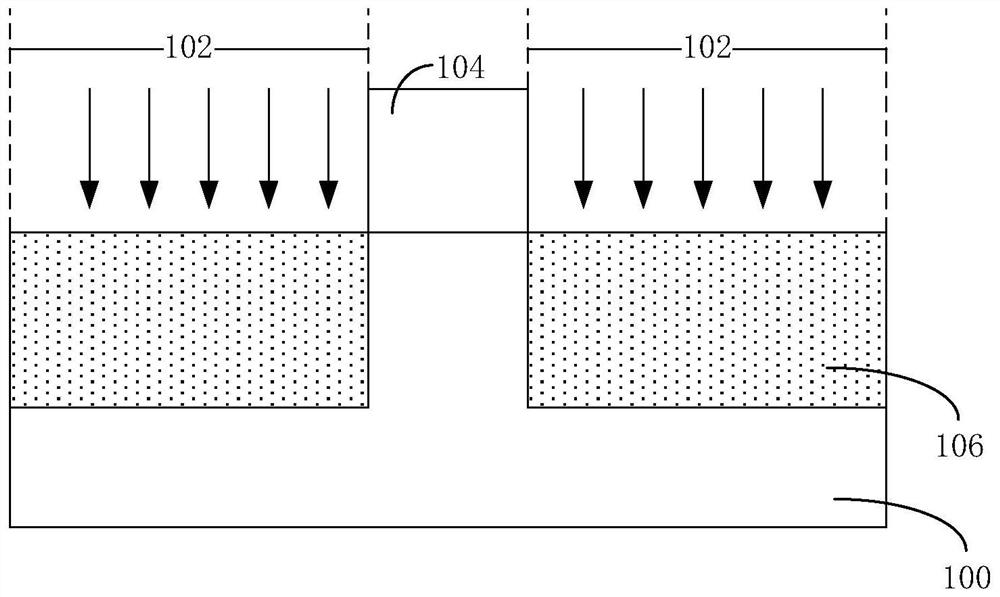
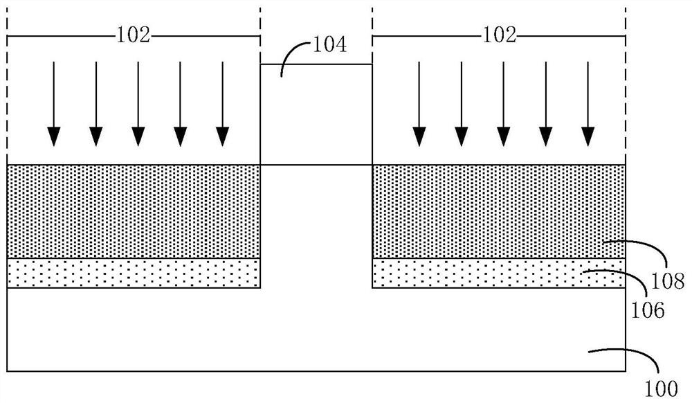
The invention relates to a preparation method of a semiconductor device, and the method comprises the steps: obtaining a substrate, and forming a gate structure on the substrate; first ion implantation is carried out on the substrate, and pre-amorphization regions are formed on the two sides of the gate structure; second ion implantation is carried out on the pre-amorphization area, and an amorphization area is formed in the pre-amorphization area; forming first side walls on two sides of the gate structure; performing a second doping process, and forming a second doped region in the non-crystallization region; second side walls are formed on the two sides of the first side walls; and forming a heavily doped source region and a heavily doped drain region in the second doped region. Transverse diffusion and longitudinal diffusion of doped ions in the second doped region are inhibited, and the effective distance between the heavily doped drain region and the edge of the drain region is increased, so that the junction leakage current is reduced.
Description
technical field [0001] The present application relates to the technical field of integrated circuits, in particular to a method for preparing a semiconductor device. Background technique [0002] With the reduction of the feature size of the semiconductor process, the size and width of the source and drain active regions of the transistor continue to shrink, resulting in the continuous increase of the series resistance of the active region of the device and the contact resistance of a single contact hole. In order to reduce the series resistance of the active region and contact resistance, after the source and drain ion implantation is completed, a metal layer is deposited on the polysilicon gate and the active area by physical vapor deposition, and then a heat treatment step is performed to make the metal layer react with the silicon in the active area and the polysilicon gate. Metal silicide is formed on the active area and the surface of the polysilicon. [0003] Compare...
Claims
Login to View More Application Information
Patent Timeline
 IPC IPC(8): H01L21/336H01L29/06H01L21/8242
CPCH01L29/66492H01L29/0607H01L29/0684H10B12/09H01L29/6659H01L29/6656H01L29/7833H01L29/1045H01L21/26506H01L21/26586H01L21/26513H01L21/28518H01L21/76855H01L21/76843H01L29/401H01L21/266
Inventor黄炜骆晓东
OwnerCHANGXIN MEMORY TECH INC