3D NAND memory based on two-dimensional material and preparation method thereof
A 3DNAND, two-dimensional material technology, applied in the semiconductor field, can solve the problems of different memory cell threshold voltage fluctuations, memory cell on-state current reduction, easy to cause reliability problems, etc., to achieve improved storage density, high on-state current, high The effect of integration
- Summary
- Abstract
- Description
- Claims
- Application Information
AI Technical Summary
Problems solved by technology
Method used
Image

Examples
Embodiment 1
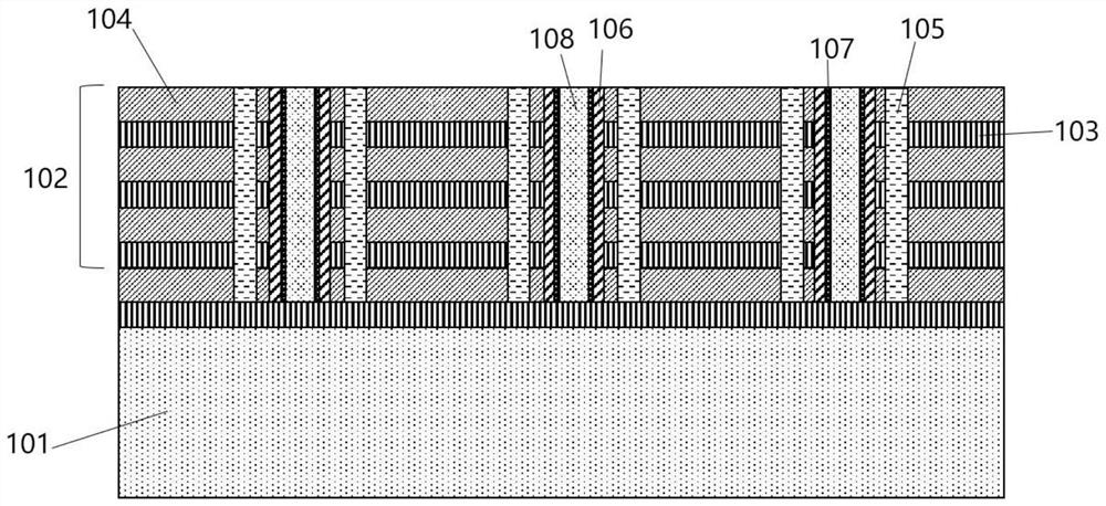
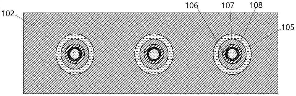
[0036] Such as figure 1 , figure 2 As shown, a 3D NAND memory based on two-dimensional materials of the present invention includes a substrate 101, a stacked structure 102, a first annular channel 105, a second annular channel 106, a channel hole 107, and a circular hole 108 ;
[0037] The stacked structure 102 is located on the upper surface of the substrate, and the stacked structure 102 is composed of a plurality of insulating layers 104 and conductive layers 103 stacked alternately, such as 32 layers, 64 layers, 256 layers and so on.
[0038] The conductive layer 103 is located on the upper surface of the substrate 101, and a first annular channel 105, a second annular channel 106, and a channel hole 107 are concentrically etched from the outside to the outside of the stacked structure 102, and The second annular channel 106 communicates with the channel hole 107, the first annular channel 105 and the second annular channel 106 are filled with an insulating medium, and ...
Embodiment 2
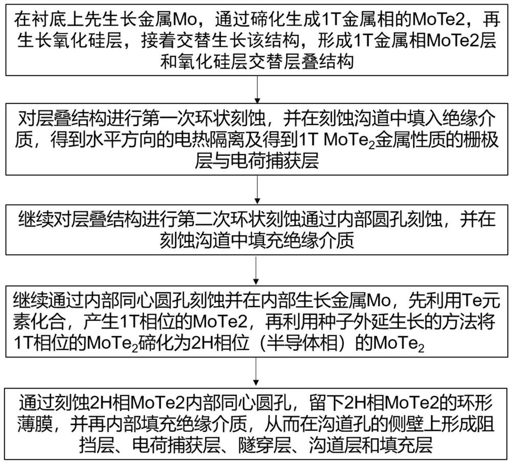
[0044] Such as image 3 Shown, a kind of preparation method of the 3D NAND memory based on two-dimensional material comprises the following steps:
[0045] Step 1, prepare the substrate 101, use the upper surface of the substrate 101 as the basal plane, grow metal Mo, and generate 1T metal phase MoTe by tellurization 2 , constitute the conductive layer 103, and then adopt a thin film deposition process to deposit and prepare a layer of silicon oxide layer on the conductive layer 103, as the insulating layer 104, and then grow repeatedly in sequence to obtain the laminated structure 102 of the conductive layer 103 and the insulating layer 104, and obtain Such as Figure 4 the structure shown;
[0046] Step 2, perform the first annular etching on the obtained laminated structure 102, and fill the insulating medium in the etched trench to obtain 1T MoTe in the horizontal direction 2 Metallic gate layer and barrier layer;
[0047] This step is to etch the laminated structure a...
PUM
 Abstract
Description
Claims
Application Information
 - Generate Ideas
- Intellectual Property
- Life Sciences
- Materials
- Tech Scout
- Unparalleled Data Quality
- Higher Quality Content
- 60% Fewer Hallucinations
Browse by: Latest US Patents, China's latest patents, Technical Efficacy Thesaurus, Application Domain, Technology Topic, Popular Technical Reports.
© 2025 PatSnap. All rights reserved.Legal|Privacy policy|Modern Slavery Act Transparency Statement|Sitemap|About US| Contact US: help@patsnap.com