Patterned composite substrate, preparation method and LED epitaxial wafer

A composite substrate and patterning technology, applied in electrical components, circuits, semiconductor devices, etc., to achieve the effects of easy etching, improved extraction rate, and increased total reflection angle

Pending Publication Date: 2022-03-18
广东中图半导体科技股份有限公司
View PDF11 Cites 1 Cited by
  • Summary
  • Abstract
  • Description
  • Claims
  • Application Information

AI Technical Summary

Problems solved by technology

On the one hand, in epitaxial growth, in order to distort the dislocations in the GaN material grown at the pattern window along the side of the pattern, and then close up on the top of the pattern, the key issue is to avoid the periodic pattern of the GaN material on the pattern substrate. Side growth, while the traditional patterned sapphire substrate (PSS) is difficult to prevent GaN material from growing on the side of its periodic pattern

Method used


Image

  • Patterned composite substrate, preparation method and LED epitaxial wafer
  • Patterned composite substrate, preparation method and LED epitaxial wafer
  • Patterned composite substrate, preparation method and LED epitaxial wafer

Examples


Embodiment Construction

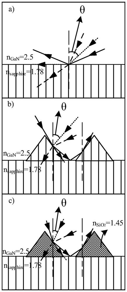
[0023] The present invention will be further described in detail below in conjunction with the accompanying drawings and embodiments. It should be understood that the specific embodiments described here are only used to explain the present invention, but not to limit the present invention. In addition, it should be noted that, for the convenience of description, only some structures related to the present invention are shown in the drawings but not all structures.

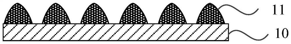
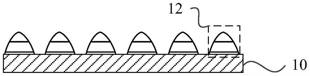
[0024] In order to further improve the light extraction rate of the patterned composite substrate, the embodiment of the present invention simulates the light paths of different substrate materials, figure 1 A schematic diagram of different substrate light path simulations provided by the embodiment of the present invention, figure 1 The substrate in a) is a sapphire flat plate, figure 1 The substrate in b) is a patterned sapphire substrate, figure 1 c) is a patterned composite substrate. figure 1 The propagati...


PUM

PropertyMeasurementUnit
thicknessaaaaaaaaaa
thicknessaaaaaaaaaa
thicknessaaaaaaaaaa

Abstract

The embodiment of the invention discloses a patterned composite substrate, a preparation method and an LED epitaxial wafer. Wherein the substrate comprises a sapphire substrate; the plurality of microstructure protrusions are located on the sapphire substrate, the microstructure protrusions comprise fluorine-doped silicon dioxide, and the refractive index of the fluorine-doped silicon dioxide is smaller than that of silicon dioxide. According to the patterned composite substrate, the preparation method thereof and the LED epitaxial wafer provided by the invention, the microstructure bulges made of the fluorine-doped silicon dioxide material are prepared above the sapphire substrate, and the refractive index of the fluorine-doped silicon dioxide material is lower, the refractive index difference between the substrate and the epitaxial layer material is larger, and the total reflection angle is increased, so that the light extraction rate can be improved; and the brightness of the epitaxial end and the chip end is improved. In addition, compared with a traditional silicon dioxide substrate material, the fluorine-doped silicon dioxide substrate material with the low refractive index is easier to etch under the same condition, the etching speed is high, the etching selection ratio is higher, and the productivity of dry etching can be improved.

Description

technical field [0001] The embodiments of the present invention relate to the field of semiconductors, and in particular to a patterned composite substrate, a preparation method and an LED epitaxial wafer. Background technique [0002] The silicon dioxide patterned composite substrate can improve the crystal quality and light extraction efficiency of GaN-based LED devices. On the one hand, in epitaxial growth, in order to distort the dislocations in the GaN material grown at the pattern window along the side of the pattern, and then close up on the top of the pattern, the key issue is to avoid the periodic pattern of the GaN material on the pattern substrate. Side growth, while the traditional patterned sapphire substrate (PSS) is difficult to prevent GaN material from growing on the side of its periodic pattern. However, the silicon dioxide patterned composite substrate has obvious advantages in this respect. Since the silicon dioxide material itself is not suitable for th...

Claims


Application Information

Patent Timeline
Patent Type & Authority Applications(China)
IPC IPC(8): H01L33/22H01L33/00H01L33/10
CPCH01L33/22H01L33/10H01L33/005
Inventor 谢鹏程陆前军张剑桥康凯吴伟杨锤
Owner 广东中图半导体科技股份有限公司
Why Eureka
Try Eureka