Preparation method of thin film and light emitting diode
A technology for light-emitting diodes and thin films, which is applied in the manufacture of semiconductor/solid-state devices, electrical components, and electrical solid-state devices. , The effect of improving the interface contact performance and reducing the interface resistance
- Summary
- Abstract
- Description
- Claims
- Application Information
AI Technical Summary
Problems solved by technology
Method used
Image

Examples
preparation example Construction
[0029] Such as figure 1 As shown, the embodiment of the present application provides a method for preparing a thin film, comprising the following steps:
[0030] S01, provide a dry film and an inert atmosphere, the inert atmosphere is doped with aromatic compounds, and the aromatic compounds can dissolve the dry film;
[0031] S02, subjecting the dry film to static treatment, heat treatment or ultraviolet light irradiation treatment under an inert atmosphere to obtain the film.
[0032] In the preparation method of the film provided in the examples of the present application, the inert atmosphere is doped with aromatic compounds capable of dissolving the dry film, and the dry film is left to stand under the inert atmosphere doped with aromatic compounds, so that the aromatic compounds are wetted In the process of dry film, it can further dissolve and disperse the large particles on the surface of the dry film, thereby improving the uniformity of the particles on the film surf...
Embodiment 1
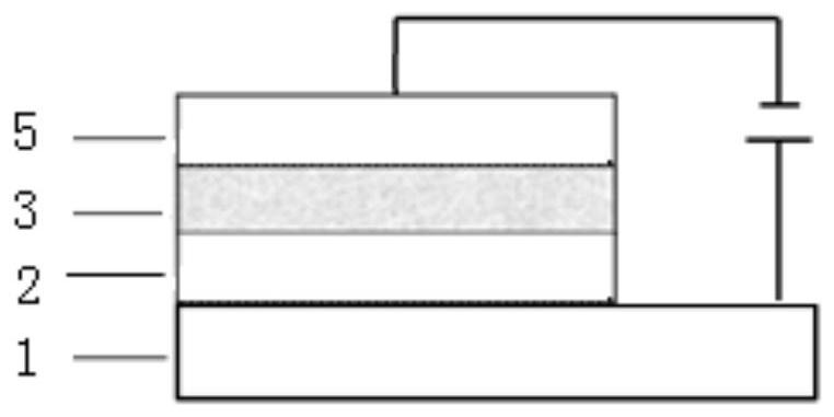
[0075] This embodiment provides a top-emitting positive quantum dot light-emitting diode, and its preparation method includes:
[0076] (1) On the ITO substrate, spin-coat PEDOT:PSS at a speed of 5000 for 30 seconds, then heat at 150°C for 15 minutes;
[0077] (2) Spin-coat TFB (8mg / mL) on the PEDOT:PSS layer at a speed of 3000 for 30 seconds, then heat at 80°C for 10 minutes;
[0078] (3) The device prepared in step (2) is put into an airtight container and left to stand for 50min, and the atmosphere environment in the airtight container is Ar atmosphere (volume concentration is 95%) and gaseous chlorobenzene (volume concentration 5%) ,Such as Figure 4 shown;
[0079] (4) the device prepared by step (3) is transferred to a glove box full of Ar atmosphere;
[0080] (5) Spin-coat quantum dots (20mg / mL) on the TFB layer at a speed of 2000 for 30 seconds;
[0081] (6) Spin-coat ZnO (30mg / mL) on the quantum dot layer at a speed of 3000 for 30 seconds, then heat at 80°C for 30...
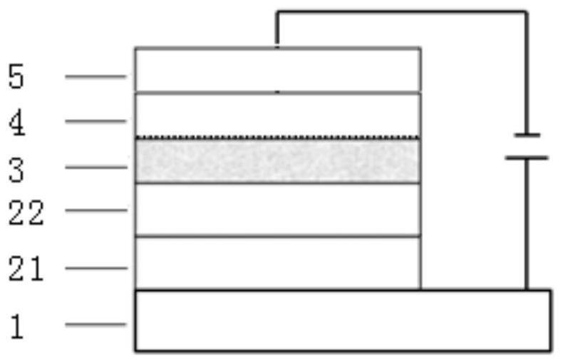
Embodiment 2
[0085]This embodiment provides a top-emitting upright quantum dot light-emitting diode, the preparation method of which is basically the same as that of Embodiment 1, the difference is that in step (2), in the mixed atmosphere filled with gaseous chlorobenzene and Ar gas TFB was spin-coated on the PEDOT:PSS layer in a glove box, where the volume concentration of gaseous chlorobenzene in the mixed atmosphere was 0.5%.
PUM
| Property | Measurement | Unit |
|---|---|---|
| Thickness | aaaaa | aaaaa |
| Thickness | aaaaa | aaaaa |
| Thickness | aaaaa | aaaaa |
Abstract
Description
Claims
Application Information
 - Generate Ideas
- Intellectual Property
- Life Sciences
- Materials
- Tech Scout
- Unparalleled Data Quality
- Higher Quality Content
- 60% Fewer Hallucinations
Browse by: Latest US Patents, China's latest patents, Technical Efficacy Thesaurus, Application Domain, Technology Topic, Popular Technical Reports.
© 2025 PatSnap. All rights reserved.Legal|Privacy policy|Modern Slavery Act Transparency Statement|Sitemap|About US| Contact US: help@patsnap.com