Chemical machine polishing method combined with rotary coating
A chemical-mechanical and spin-coating technology, applied in the direction of grinding devices, grinding machine tools, machine tools suitable for grinding workpiece planes, etc., can solve the silicon dioxide layer pollution of the wafer, the relative effect is not as expected, and it does not have self-flatness Problems such as chemical function, to achieve the effect of thin grinding sacrificial layer thickness
- Summary
- Abstract
- Description
- Claims
- Application Information
AI Technical Summary
Problems solved by technology
Method used
Image
Examples
Embodiment 1
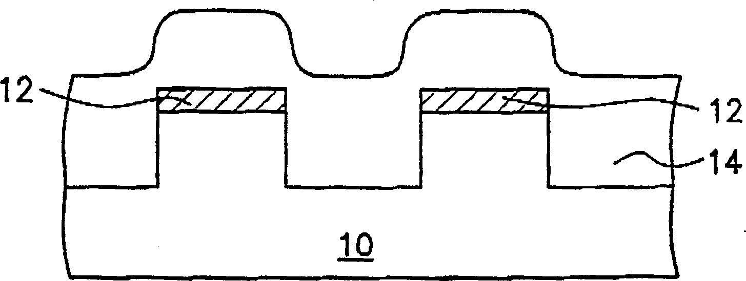
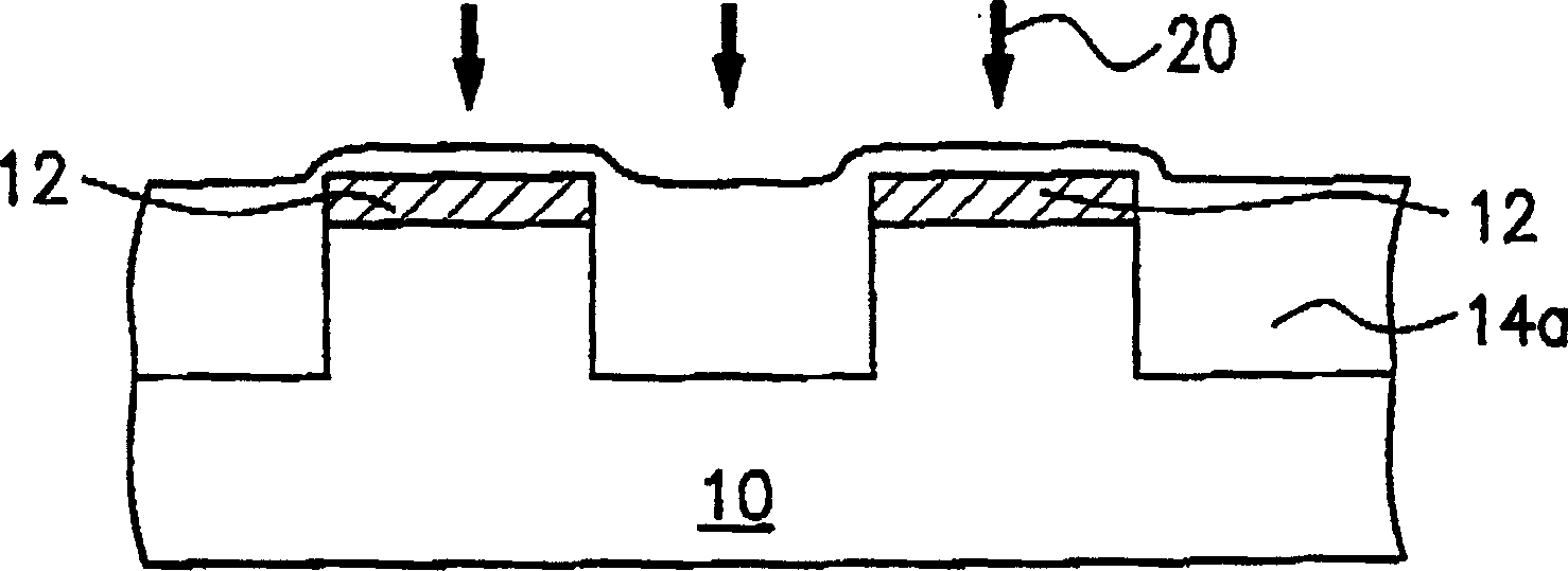
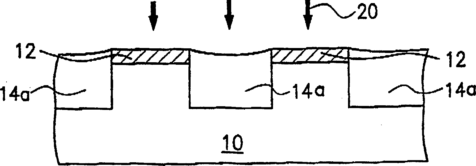
[0030] Figure 2A to Figure 2C It is a schematic cross-sectional view of a chemical mechanical polishing method combined with spin coating according to the first preferred embodiment of the present invention.
[0031] Taking the formation of shallow trench isolation regions as an example, please refer to Figure 2A, forming an insulating layer on the semiconductor substrate 100, this step is, for example, depositing a silicon nitride layer by chemical vapor deposition. Secondly, the shallow trench isolation method is carried out, that is, the component area and the isolation area are defined through lithography and etching steps, and one or two layers are deposited by chemical vapor deposition on the recessed isolation area and the stop layer 112 on the component area. Silicon oxide layer 114 . Next, on the entire semiconductor substrate 100 , a spin-coating material layer 116 is formed by spin-coating and cured, so that the height difference between the device area and the ...
Embodiment 2
[0035] Figure 3A to Figure 3C It is a schematic cross-sectional view of a chemical mechanical polishing method combined with spin coating according to the second preferred embodiment of the present invention.
[0036] To form a dielectric layer between conductive layers as an example, please refer to Figure 3A , on the semiconductor substrate 200 to be planarized and on the conductive layer 213, a silicon dioxide layer 214 is deposited by chemical vapor deposition. Then, on the entire semiconductor substrate 200 , a spin coating material layer 216 is formed by spin coating and cured, so that the height difference between the conductive layers 213 and the conductive layers 213 will not be too large. The spin coating is preferably made of silica glass or silica glass or polymer doped with a polymer, and the thickness of the formed spin coating material layer is about 2000 angstroms to 7000 angstroms.
[0037] Please refer to Figure 3B , transfer the wafer to a polishing pa...
Embodiment 3
[0040] Figure 4A to Figure 4C It is a schematic cross-sectional view of a chemical mechanical polishing method combined with spin coating according to the third preferred embodiment of the present invention.
[0041] To form a dielectric layer between conductive layers as an example, please refer to Figure 4A , on the semiconductor substrate 300 to be planarized and on the conductive layer 313, a silicon dioxide layer 314 is deposited by chemical vapor deposition. Then on the whole semiconductor substrate 300, after forming a first spin coating material layer 316 by spin coating and curing, and then forming a second spin coating material layer 318 by spin coating and curing, the conductive layer The height difference between 313 and the conductive layer 313 will not be too large. The spin coating is preferably made of silica glass or silica glass or polymer doped with a polymer, and the thickness of the formed spin coating material layer is about 2000 angstroms to 7000 ang...
PUM
| Property | Measurement | Unit |
|---|---|---|
| thickness | aaaaa | aaaaa |
Abstract
Description
Claims
Application Information
 - R&D Engineer
- R&D Manager
- IP Professional
- Industry Leading Data Capabilities
- Powerful AI technology
- Patent DNA Extraction
Browse by: Latest US Patents, China's latest patents, Technical Efficacy Thesaurus, Application Domain, Technology Topic, Popular Technical Reports.
© 2024 PatSnap. All rights reserved.Legal|Privacy policy|Modern Slavery Act Transparency Statement|Sitemap|About US| Contact US: help@patsnap.com


