Silicon carbide MPS diode with buried layer structure and preparation method thereof

A technology of silicon carbide and diodes, which is applied in the field of silicon carbide MPS diodes and its preparation, can solve problems such as diode failure and large PN junction conduction voltage, achieve high-current operating temperature reduction, reduce conduction resistance, and improve surge resistance The effect of current capacity

Pending Publication Date: 2022-04-01
安徽长飞先进半导体有限公司
View PDF0 Cites 1 Cited by
  • Summary
  • Abstract
  • Description
  • Claims
  • Application Information

AI Technical Summary

Problems solved by technology

In order to ensure that the working current under normal operation meets the requirements, usually the PN junction area accounts for a small proportion of the total chip area. Due to the small proportion of the P

Method used


Image

  • Silicon carbide MPS diode with buried layer structure and preparation method thereof
  • Silicon carbide MPS diode with buried layer structure and preparation method thereof
  • Silicon carbide MPS diode with buried layer structure and preparation method thereof

Examples


Embodiment Construction

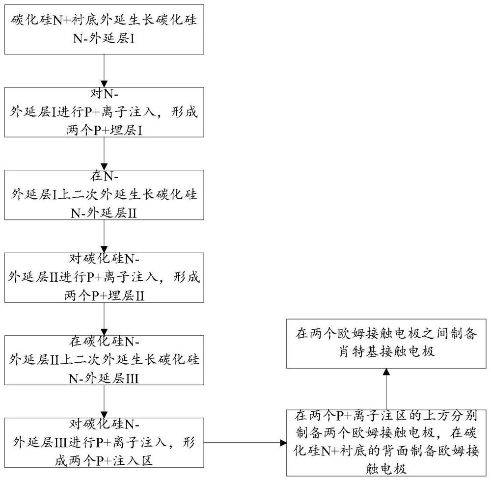
[0032] The specific implementation of the present invention will be described in further detail below by describing the embodiments with reference to the accompanying drawings, so as to help those skilled in the art have a more complete, accurate and in-depth understanding of the inventive concepts and technical solutions of the present invention.

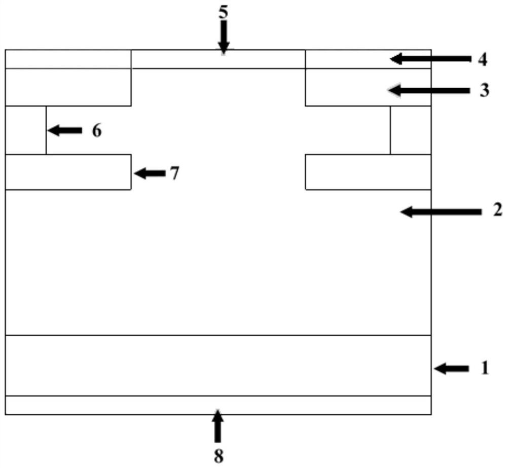
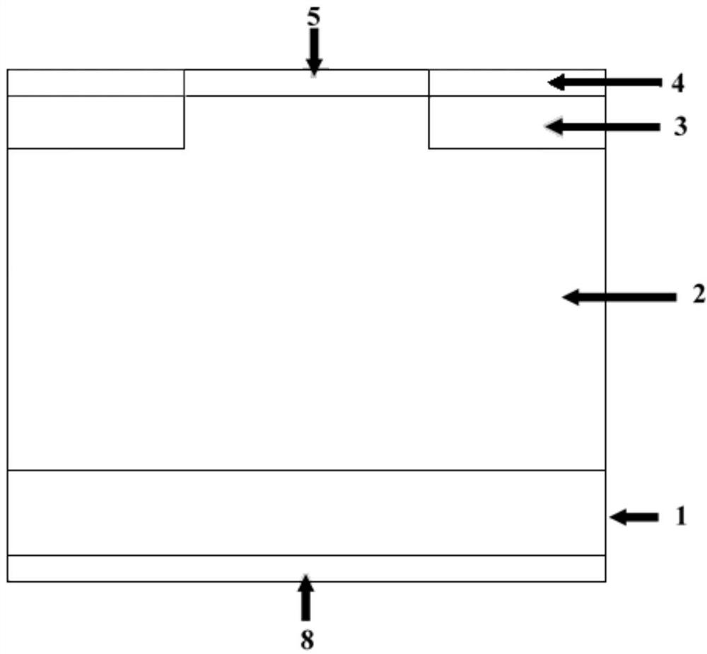
[0033] figure 1 The structure schematic diagram of the silicon carbide MPS diode with buried layer structure provided by the present invention, for the convenience of description, only shows the part related to the embodiment of the present invention.

[0034] The SiC MPS Diode includes:

[0035] A cathode ohmic contact electrode (8), a silicon carbide N+ substrate (1) and a silicon carbide N- epitaxial layer (2) stacked from bottom to top;

[0036] Two P+ implantation regions (3) are formed on the top of the silicon carbide N- epitaxial layer (2), the bottoms of the two P+ implantation regions (3) are in contact with the tops of ...


PUM


Abstract

The silicon carbide MPS diode comprises a cathode ohmic contact electrode, a silicon carbide N + substrate and a silicon carbide N-epitaxial layer which are laminated from bottom to top, two P + injection regions are formed at the top of the silicon carbide N-epitaxial layer, the two P + injection regions are respectively contacted with the tops of the two P + buried layers I through the two P + buried layers II, and the widths of the P + injection regions and the P + buried layers I are greater than those of the P + buried layers II; two ohmic contact electrodes are arranged at the tops of the two P + injection regions, and a Schottky contact electrode is arranged between the two ohmic contact electrodes. The P + injection region and the P + buried layer I are connected through the narrow P + buried layer II, the proportion of PN junctions is increased in the epitaxial layer, and the snapback phenomenon during forward conduction of the MPS diode is eliminated; and meanwhile, the breakover voltage of the MPS diode from a unipolar working state to a bipolar working state is reduced, so that the diode enters the bipolar working state under a relatively low forward current, the high-current working temperature of the diode is reduced, and higher surge current resistance is achieved.

Description

technical field [0001] The invention belongs to the technical field of semiconductors, and more specifically, the invention relates to a silicon carbide MPS diode with a buried layer structure and a preparation method thereof. Background technique [0002] The third-generation wide-bandgap semiconductor material silicon carbide relies on its excellent material physical and electrical properties. For example, compared with silicon (Si) materials, silicon carbide (4H-SiC) has a wide band gap (3 times that of Si) and high electron saturation. Significant advantages such as drift speed (2.5 times that of Si), high thermal conductivity (3.3 times that of Si), high critical breakdown electric field (10 times that of Si), can operate at high power density, high frequency and high temperature, and conduct The loss during switching and switching is also lower, especially suitable for the preparation of semiconductor power devices with high voltage resistance, high power, radiation re...

Claims


Application Information

Patent Timeline
IPC IPC(8): H01L29/06H01L29/868H01L29/872H01L21/329
Inventor 罗茂久邢婷婷钮应喜袁松彭强乔庆楠
Owner 安徽长飞先进半导体有限公司
Why Eureka
Try Eureka