Preparation process of high-strength integrally-formed micro-inductor

A preparation process and micro-inductance technology, applied in the field of microelectronics, can solve the problems of affecting micro-inductance, non-conductive resistance, easy to break under force, etc.

Active Publication Date: 2022-04-12
华萃微感电子(江苏)有限公司
View PDF7 Cites 0 Cited by
  • Summary
  • Abstract
  • Description
  • Claims
  • Application Information

AI Technical Summary

Problems solved by technology

In order to increase the series inductance, increase the quality factor, reduce the volume, reduce the loss, etc., many technologies have been used, such as photolithography, sputtering, electroplating, etc., because th...

Method used


Image

  • Preparation process of high-strength integrally-formed micro-inductor
  • Preparation process of high-strength integrally-formed micro-inductor

Examples


Embodiment 1

[0029] A high-strength integral molding micro-inductor preparation process, the high-strength integral molding micro-inductance preparation process mainly includes the following preparation steps:

[0030] (1) Coil production: under the conditions of pressure 1Pa, argon gas flow rate 15sccn, sputtering power 100w, sputtering rate 4nm / min, temperature 20°C, sputter 0.3μm on a smooth silicon dioxide substrate by magnetron sputtering For a thick chromium layer, spin-coat photoresist AZ P4620 to a thickness of 4 μm on the chromium layer at 3000r / min, and then stand at 20°C for 20min, 50°C for 60min, 90°C for 6h, and 110°C for 60min. Baking, cooling to 20°C, covering the photoresist with a photomask for contact exposure, exposure time 60s, then immersing in pure water at 20°C for 5 minutes to develop, cleaning the surface with absolute ethanol for 3 times, at 350g / L Copper plating is carried out in an electroplating solution of copper sulfate and 30mL / L sulfuric acid, at a current ...

Embodiment 2

[0035] A high-strength integral molding micro-inductor preparation process, the high-strength integral molding micro-inductance preparation process mainly includes the following preparation steps:

[0036] (1) Coil production: under the conditions of pressure 2Pa, argon gas flow rate 18sccn, sputtering power 120w, sputtering rate 5nm / min, temperature 25°C, sputter 0.4μm on a smooth silicon dioxide substrate by magnetron sputtering For a thick chromium layer, spin-coat photoresist AZ P4620 to a thickness of 5 μm on the chromium layer at 3500r / min, and then stand at 25°C for 18min, 55°C for 55min, 95°C for 4h, and 115°C for 50min. Baking, cooling to 25°C, covering the photoresist with a photomask for contact exposure, exposure time 55s, then immersing in pure water at 25°C for 4 minutes to develop, cleaning the surface 4 times with absolute ethanol, at 350g / L Copper plating is carried out in an electroplating solution of copper sulfate and 30mL / L sulfuric acid, at a current dens...

Embodiment 3

[0041] A high-strength integral molding micro-inductor preparation process, the high-strength integral molding micro-inductance preparation process mainly includes the following preparation steps:

[0042] (1) Coil production: under the conditions of pressure 3Pa, argon gas flow rate 20sccn, sputtering power 150w, sputtering rate 6nm / min, temperature 30°C, magnetron sputtering is sputtering 0.5μm on a smooth silicon dioxide substrate For a thick chromium layer, spin-coat photoresist AZ P4620 to a thickness of 6 μm at 4000 r / min on the chromium layer, and then stand at 30°C for 15 minutes, 60°C for 50 minutes, 100°C for 5 hours, and 120°C for 40 minutes. Baking, cooling to 30°C, covering the photoresist with a photomask for contact exposure, exposure time 50s, then immersing in pure water at 30°C for 3 minutes to develop, cleaning the surface with absolute ethanol 5 times, at 350g / L Copper plating is carried out in an electroplating solution of copper sulfate and 30mL / L sulfuri...


PUM


Abstract

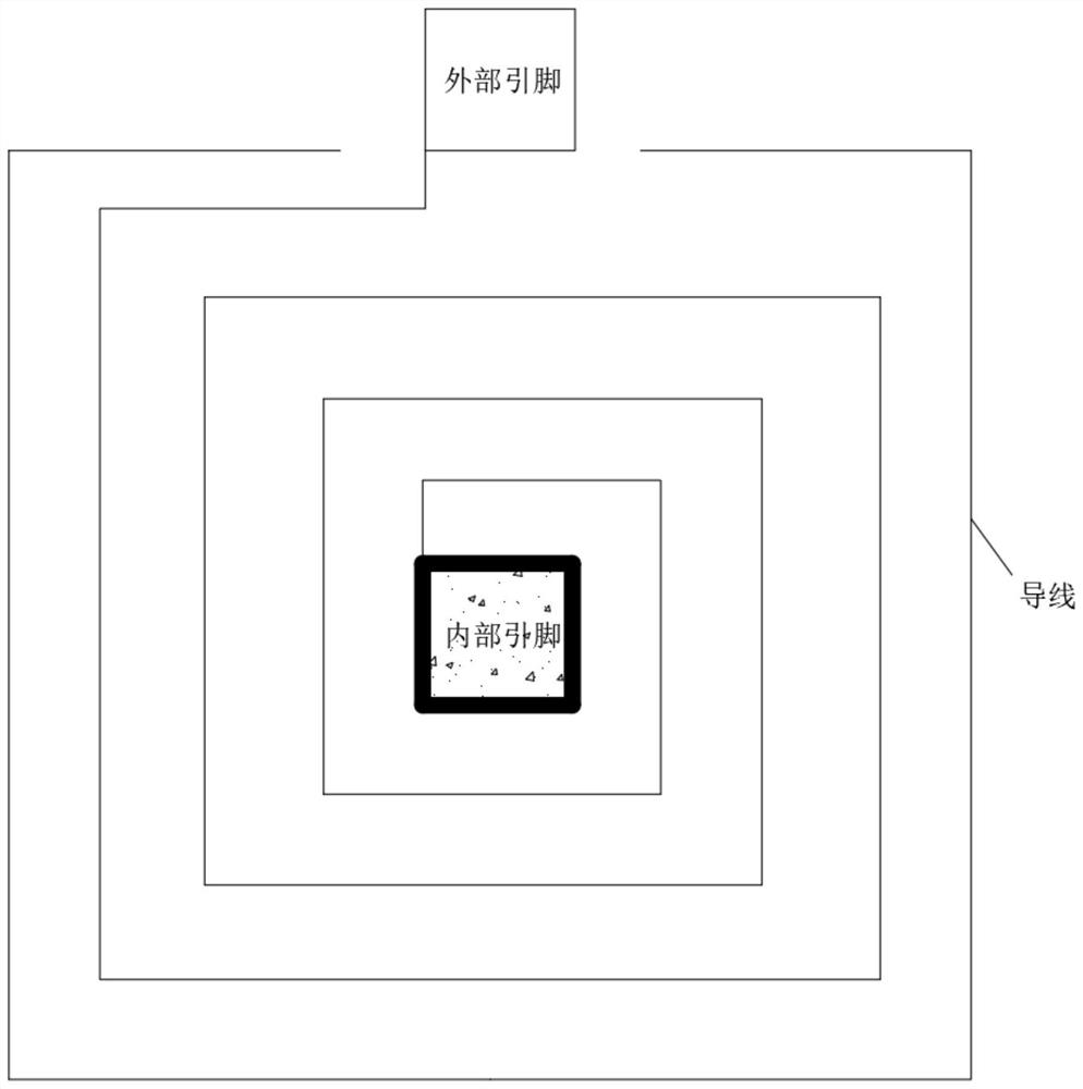
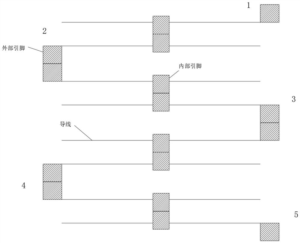
The invention discloses a preparation process of a high-strength integrally-formed micro inductor, and relates to the technical field of microelectronics. When the high-strength integrally-formed micro-inductor is prepared, firstly, a coil is manufactured to obtain a hollow-core rectangular coil with protruding external pins, then primary protection is conducted, the external pins are made to protrude to form a single-layer planar micro-inductor, a semi-finished micro-inductor is manufactured through assembling, and 3, 4, 5-trimethyl-1, 3, 5-trimethyl-1, 3, 5-trimethyl-1, 3, 5-trimethyl-1, 3, 5-trimethyl-1, 3, 5-trimethyl-1, 3, 5-trimethyl-1, 3, 5 the modified organic silica gel forms porous protection columns at the two ends of an external pin through secondary protection, and the high-strength integrally-formed micro inductor is manufactured. The prepared aluminum nitride has good stress protection performance and oxidation corrosion resistance, and is easy to install and use.

Description

technical field [0001] The invention relates to the technical field of microelectronics, in particular to a high-strength integral molding micro-inductor preparation process. Background technique [0002] The transformative development of microelectronics technology and semiconductor technology has promoted the rapid development of information technology. The super-integration of electronic devices is an inevitable trend of development. Electronic components are developing toward "small, light, thin, and fine", and micro-inductance components are also bound to The development of miniaturization, high frequency, array, integration and high performance. [0003] Microinductors, as the core components of MEMS devices and core devices of integrated circuit chips, can be widely used in the fields of communication, home appliances, sensing, aerospace and voltage transformation. In order to increase the series inductance, increase the quality factor, reduce the volume, reduce the ...

Claims


Application Information

Patent Timeline
IPC IPC(8): H01F41/04H01F41/00
Inventor 高彦华周晟
Owner 华萃微感电子(江苏)有限公司
Why Eureka
Try Eureka