Device for LED wafer manufacturing process

A wafer and process technology, applied in the field of LED wafer process equipment, can solve problems such as machine failure, large pressure ring size of the carrier plate, and inability to press the carrier plate, etc., to ensure wafer processing yield, The effect of reducing the area of ​​the slot and increasing the number

Pending Publication Date: 2022-04-12
XIAMEN CHANGELIGHT CO LTD
View PDF0 Cites 0 Cited by
  • Summary
  • Abstract
  • Description
  • Claims
  • Application Information

AI Technical Summary

Problems solved by technology

[0005] In view of this, the present invention provides a device for LED wafer manufacturing process. While appropriately increasing the size of the carrier plate, a small-scale modification of the pressure ring of the PVD machine is carried out to solve the problem of increasing the carrier plate in order to increase production capacity in the background technology. The size of the carrier plate is too large and the size of the pressure ring of the PVD machine does not match, and the pressure ring cannot press the carrier plate, resulting in the problem that the machine cannot work normally.

Method used


Image

  • Device for LED wafer manufacturing process
  • Device for LED wafer manufacturing process
  • Device for LED wafer manufacturing process

Examples


Embodiment 1

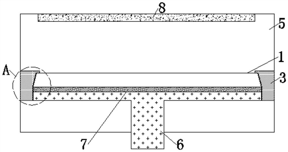
[0043] A device for LED wafer manufacturing process provided by this embodiment, such as image 3 , Figure 4 shown, including:

[0044] Carrier 1, the carrier 1 is provided with a wafer placement surface, the side 2 of the carrier is an inclined surface, and the side 2 of the carrier forms a carrier inclination angle θ1 with the wafer placement surface;

[0045] The pressing ring 3, the pressing ring 3 includes a pressing part 31 and a positioning angle θ2 of the pressing ring;

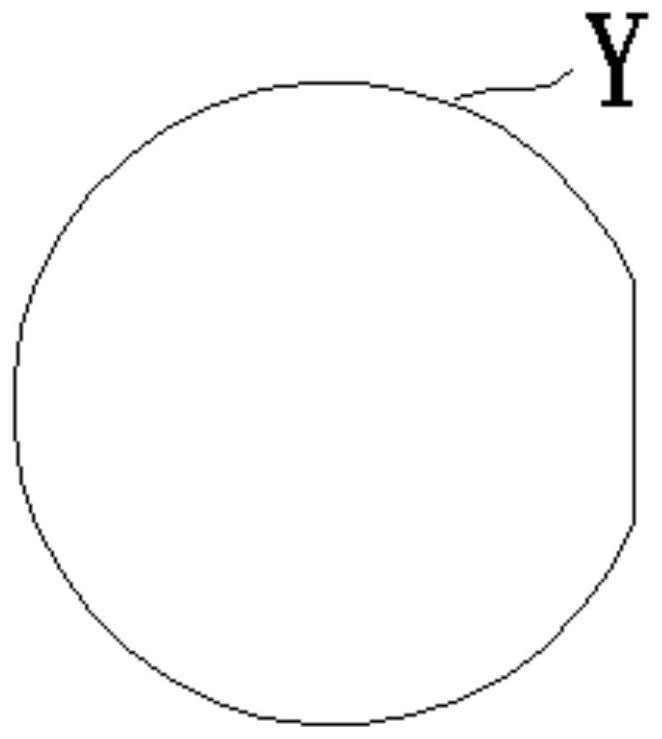
[0046] During the LED wafer manufacturing process, the wafer Y is placed on the wafer placement surface, the pressure ring 3 is used to fix the carrier plate 1, the pressure ring positioning angle θ2 is used to position the carrier plate inclination angle θ1, and the pressing part 31 is used to press the carrier plate Edge 4, wherein the shape and angle of the positioning angle θ2 of the pressure ring matches the inclination angle θ1 of the carrier plate.

[0047] It should be noted that during th...

Embodiment 2

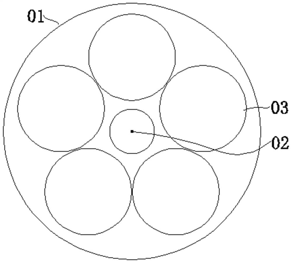
[0050] Such as Figure 5 , Figure 6 As shown, a device for LED wafer manufacturing process differs from the first embodiment above in that the wafer placement surface is provided with wafer placement grooves 9 close to each other; the wafer placement groove 9 includes a central wafer placement Slot 91 and several peripheral wafer placement slots 92; the central wafer placement slot 91 is located at the center of the wafer placement surface, and each peripheral wafer placement slot 92 is set around the center wafer placement slot 91.

[0051] Optionally, in this embodiment, the bottom surfaces of the wafer placement slots 9 are at the same level.

[0052] Optionally, in this embodiment, the width W1 of the side surface of the carrier plate in the vertical direction ranges from 1 mm to 3 mm, inclusive.

[0053] Optionally, in this embodiment, the edge width W2 of the carrier plate ranges from 2 mm to 10 mm, including the endpoints.

[0054] Optionally, in this embodiment, th...

Embodiment 3

[0058] Such as Figure 7 As shown, a device for LED wafer manufacturing process differs from the second embodiment above in that the raised portion between the central wafer placement groove 91 and the peripheral wafer placement groove 92 is the Y region 10, and the peripheral wafer The raised portion between the circular placement groove 92 and the side surface 2 of the carrier plate is the Z zone 11; the horizontal height of the bottom surface of the central wafer placement groove is H1, the horizontal height of the Y zone is H2, the horizontal height of the Z zone is H3, and the wafer height is H4 , then H1<H2≤H1+H4, and H2<H3.

[0059] It should be noted that, in this embodiment, the edge 4 of the carrier disk (not shown in the figure) is within the range of the Z zone 11 .

[0060] Optionally, in this embodiment, the level difference between H2 and H1 ranges from 20 um to 650 um, including the endpoint values.

[0061] Optionally, in this embodiment, pick-and-place open...


PUM

PropertyMeasurementUnit
Edge widthaaaaaaaaaa
Diameteraaaaaaaaaa
The inside diameter ofaaaaaaaaaa

Abstract

The invention provides a device for LED wafer processing, which comprises a carrying disc and a pressing ring, the side surface of the carrying disc is an inclined surface, a carrying disc inclination angle is formed between the side surface of the carrying disc and a wafer placing surface, the pressing ring is used for fixing the carrying disc, a pressing ring positioning angle is used for positioning the carrying disc inclination angle, and a sheet pressing part is used for pressing the edge of the carrying disc. The shape and the angle of the press ring positioning angle are matched with the shape and the angle of the carrier plate inclination angle, the size of the carrier plate is properly increased, meanwhile, the problem that the press ring cannot press the carrier plate due to the fact that the carrier plate is too large is avoided, a machine table can work normally, and the phenomenon that the carrier plate is prone to deviating from fixation of the press ring in the process that the carrier plate is conveyed into a cavity in the manufacturing process and rubs with the press ring can be avoided. The service life of the carrying disc and the wafer processing yield can be effectively guaranteed, and stable large-scale mass production is achieved.

Description

technical field [0001] The invention belongs to the technical field of semiconductors, and more specifically relates to a device for LED wafer manufacturing process. Background technique [0002] III-V nitrides, due to their direct bandgap semiconductor characteristics, have excellent physical properties such as large forbidden band width, high breakdown electric field, and high electron saturation mobility, and have received extensive attention in the fields of electronics and optics. Among them, GaN-based light-emitting diodes have made great progress in lighting, display, and digital. Studies have shown that using PVD (Physical Vapor Deposition, physical vapor deposition) to evaporate a layer of AlN buffer layer on the sapphire substrate, and then epitaxial GaN material can significantly improve the quality of GaN-based LED crystals, thereby significantly improving the performance of LED devices. This processing technology of patterned sapphire substrate combined with va...

Claims


Application Information

Patent Timeline
IPC IPC(8): H01L21/673H01L21/687H01L33/00C23C14/02C23C14/06C23C14/24C23C14/50
Inventor 林志园洪金居梁基麟陈龙陈乐崔恒平蔡玉梅蔡海防
Owner XIAMEN CHANGELIGHT CO LTD
Why Eureka
Try Eureka