Shield gate groove type field effect transistor based on charge compensation and preparation method thereof
A technology of field effect transistor and charge compensation, which is applied in the field of shielded gate trench type field effect transistor and its preparation, can solve the problems of reducing transmission capacitance, achieve low on-resistance, prevent breakdown, and reduce on-resistance Effect
- Summary
- Abstract
- Description
- Claims
- Application Information
AI Technical Summary
Problems solved by technology
Method used
Image

Examples
Embodiment 1
[0051]In a traditional SGT device, when the SGT device is off, the drift region is a withstand voltage region. When the device is at withstand voltage, the electric force lines generated by the ionized donor positive charges in the drift region are terminated to the trench shielded gate. At this time, due to the electric field concentration effect, the electric field lines in the drift region are concentrated near the shield gate, and the corners of the trench region bear a strong electric field, which often causes the transistor to be broken down between the drift region and the trench region. Therefore, in order to avoid the generation of a strong electric field at the corner of the trench region due to the electric field concentration effect and improve the breakdown voltage of the transistor, it is urgent to design a new shielded gate trench field effect transistor. An embodiment of the present application provides a shielded gate trench field effect transistor based on ch...
Embodiment 2
[0067] Based on the shielded gate trench field effect transistor based on charge compensation described in Embodiment 1, since the base region is short-circuited with the N-type source region connected to the channel through the heavily doped P-type source region, when the SGT is in the forward direction When blocking or when the voltage between the drain and the source is high, the transistor generates holes due to the avalanche effect, and flows through the channel in the base region to form a hole current that prompts the parasitic triode to turn on. The hole current flows through the channel of the body region, causing the parasitic triode to be turned on, and the turning on of the parasitic triode will lead to avalanche failure of the transistor.
[0068] In order to delay the turn-on of the parasitic transistor, the embodiment of the present application also provides another shielded gate trench field effect transistor based on charge compensation.
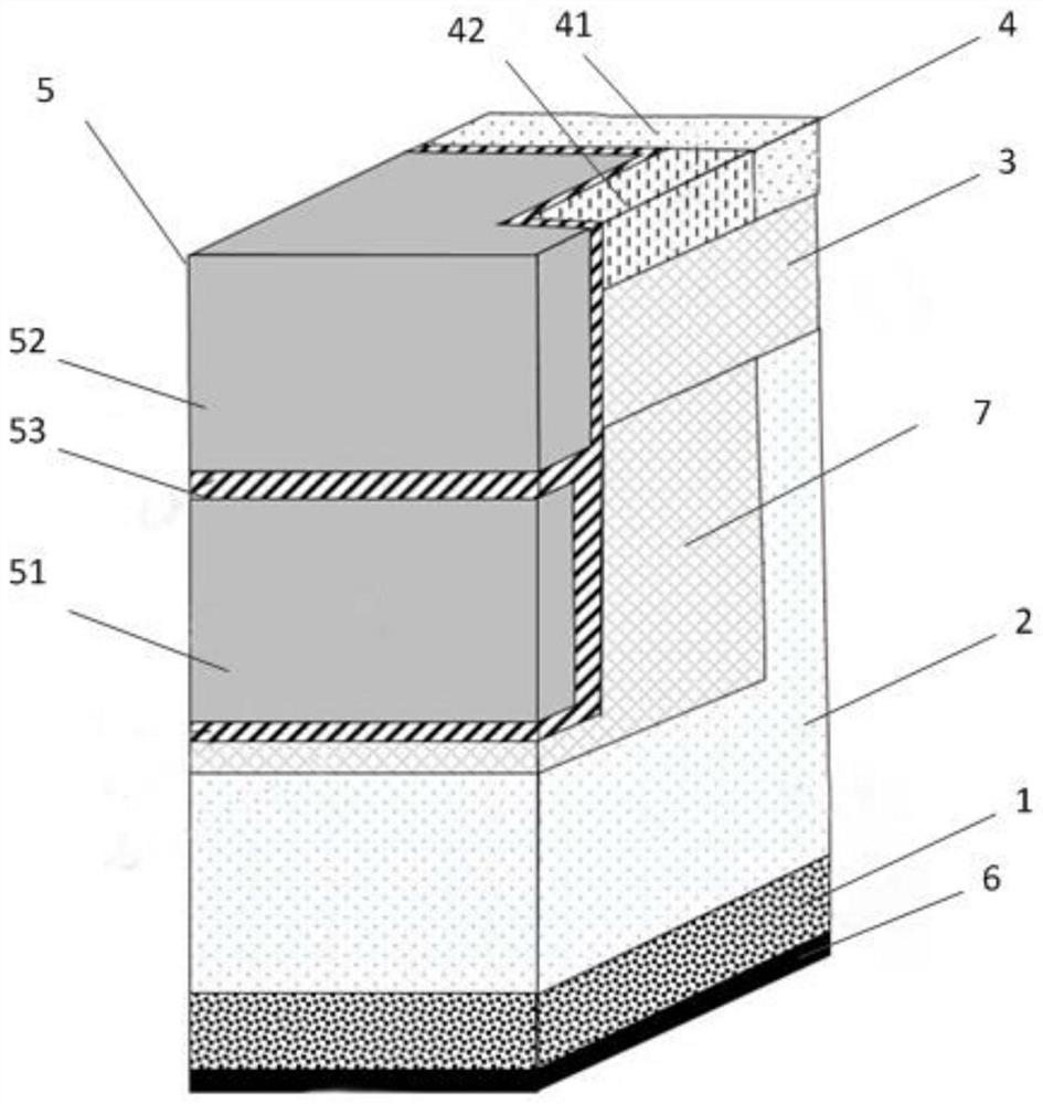
[0069] figure 1 It ...
Embodiment 3
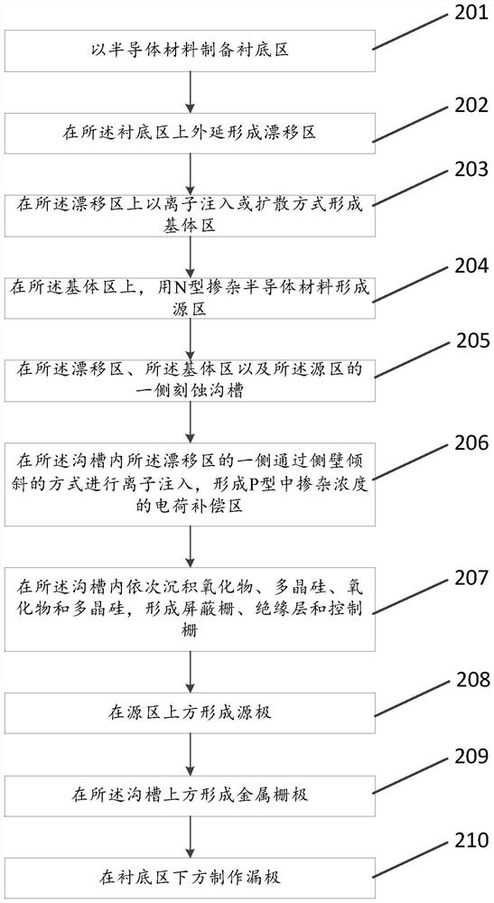
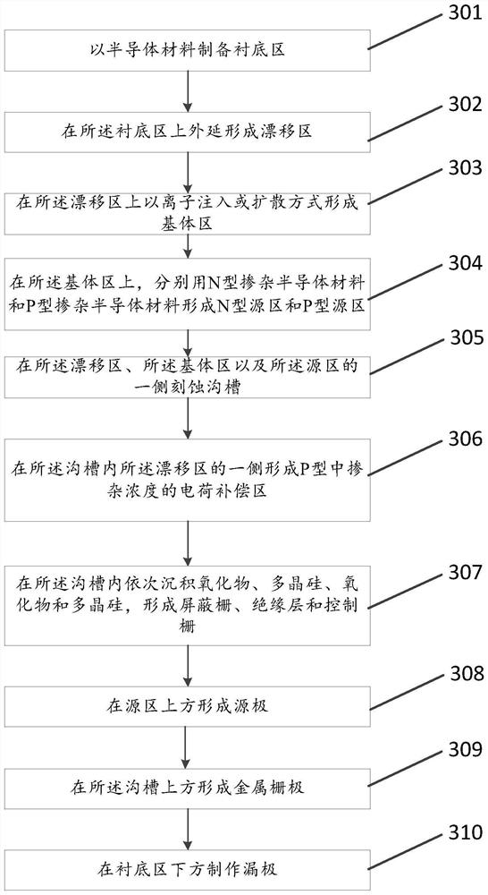
[0086] Corresponding to the shielded gate trench field effect transistor based on charge compensation shown in Embodiment 1, the present application also provides a preparation method of a shielded gate trench field effect transistor based on charge compensation and the corresponding embodiment .
[0087] figure 2 It is a schematic flowchart of a method for manufacturing a shielded gate trench field effect transistor based on charge compensation shown in an embodiment of the present application.
[0088] see figure 2 , the preparation method of the shielded gate trench type field effect transistor, comprising:
[0089] 201. Prepare a substrate region with a semiconductor material;
[0090] In the embodiment of the present application, the substrate region is prepared with an N-type heavily doped semiconductor material, that is, the doping type of the substrate region is N-type doping, and the doping concentration of the substrate region is a heavily doped concentration. ...
PUM
 Abstract
Description
Claims
Application Information
 - R&D
- Intellectual Property
- Life Sciences
- Materials
- Tech Scout
- Unparalleled Data Quality
- Higher Quality Content
- 60% Fewer Hallucinations
Browse by: Latest US Patents, China's latest patents, Technical Efficacy Thesaurus, Application Domain, Technology Topic, Popular Technical Reports.
© 2025 PatSnap. All rights reserved.Legal|Privacy policy|Modern Slavery Act Transparency Statement|Sitemap|About US| Contact US: help@patsnap.com