Antenna device

An antenna device and antenna technology, applied in the field of antenna manufacturing, to achieve the effect of alleviating component constant changes

Pending Publication Date: 2022-04-19
SHANDONG HUALING ELECTRONICS
View PDF3 Cites 0 Cited by
  • Summary
  • Abstract
  • Description
  • Claims
  • Application Information

AI Technical Summary

Problems solved by technology

[0007] The content described in Patent Document 3 focuses on the pressure change caused by the temperature difference between the inside and the outside. Although the interval between the patch antenna 61 and the passive

Method used


Image

  • Antenna device
  • Antenna device
  • Antenna device

Examples


Embodiment 1

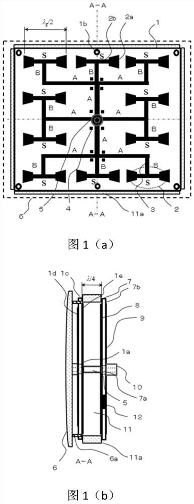
[0028] figure 1 It is a plan view and a cross-sectional view of an antenna device composed of a parallel feeding type array according to Embodiment 1 of the present invention. figure 1 Among them, the first dielectric substrate 1 is provided with a large hole (1a) in the central part, and a small hole (1b) is provided in the peripheral part. The insulating layer 1c is a liquid crystal polymer-(FCP) material; a copper foil pattern 1d is formed on one surface, and the other One surface (back side) is used as ground pattern (ground conductor part) 1e; Antenna part 2 is made of conical antenna pattern 2a and rectangular elongated antenna pattern 2b that expand towards the figure front end, and the center of elongated antenna pattern 2b is connected with transmission line 3, S indicates a branch located at the center of the antenna pattern 2b.

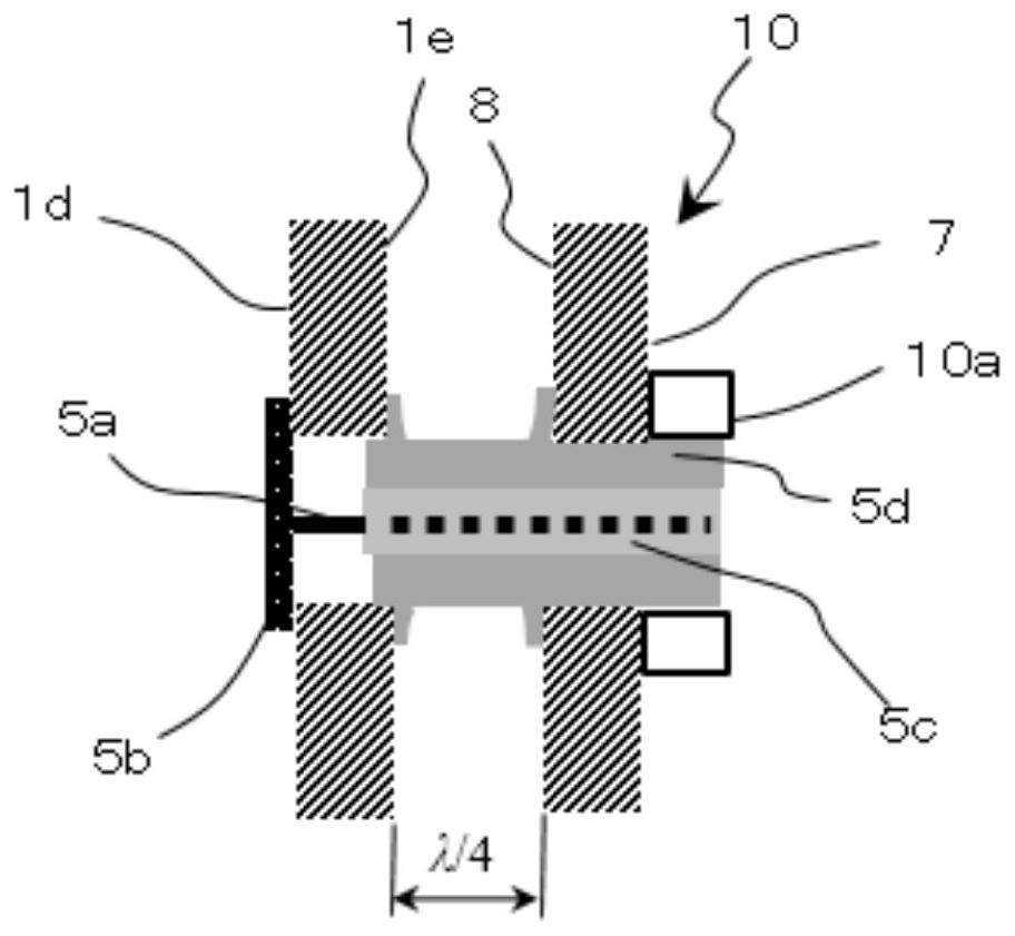
[0029] Assuming that the central position of the first dielectric substrate 1 is the feeding section 5, the length of each transmission l...

Embodiment 2

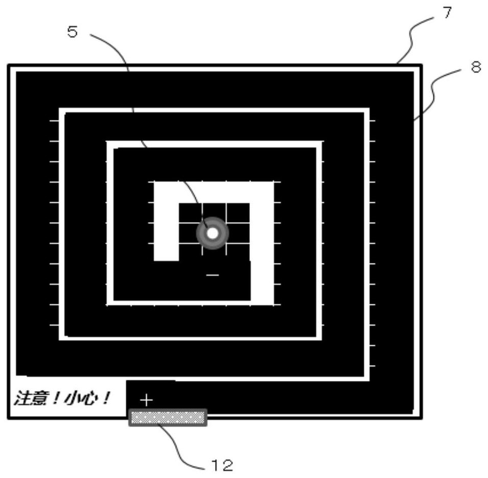
[0044] Figure 5 is a schematic diagram of the structure of the reflector of the antenna device according to Embodiment 2 of the present invention. exist figure 2 Among them, a vortex-shaped heating part 8 is provided. When the sheet resistance value of the heating part is low, the desired resistance value can be obtained by bending the pattern multiple times in a Mianda shape. island pattern, thereby maintaining the function of the high-frequency reflector.

[0045] As described above, according to the antenna device according to Embodiment 2, the thermal insulation wall for the space between the first dielectric on which the antenna is mounted and the second dielectric substrate opposite to each other is provided, and the reflector of the second dielectric substrate is provided to adjust the temperature in the space. Since the heat-generating part of the pattern covers the entire surface of the reflector, it has the effect of maintaining the function of the reflector.

Embodiment 3

[0047] Image 6 It is a schematic plan view showing the structure of the reflector of the antenna device according to Embodiment 3 of the present invention. exist figure 1 Among them, the heat generated by the space part 11 is radiation heating, and in Image 6 In the space part 11, the filling resin that can pass high-frequency signals is used as the sealing part 110 for conduction heating; as mentioned above, according to the antenna device of Embodiment 3 of the present invention, the resin that can pass high-frequency signals is filled in In the heat-retaining wall 11a, the heat-retaining time becomes longer, and by contacting the heat-generating portion 8, the effect of protecting the surface of the heat-generating portion 8 can be achieved at the same time.

[0048] The antenna device proposed by the present invention has the function of reducing the accompanying heat loss due to the heat insulation wall covering the space between the first dielectric substrate on whic...


PUM

PropertyMeasurementUnit
Resistanceaaaaaaaaaa

Abstract

The invention relates to the technical field of antenna manufacturing, in particular to an antenna device which is small in size, compact in structure and capable of forming an antenna loop on a planar substrate, antenna characteristics of the antenna device do not change along with dramatic changes of environment temperature, and the antenna device comprises a first dielectric substrate which is provided with an antenna part. The high-power microstrip antenna is characterized in that a heating part is arranged on the surface, facing the back face of the first dielectric substrate, of the second dielectric substrate, and an air heat preservation layer is formed between the first dielectric substrate and the second dielectric substrate; the first dielectric substrate and the second dielectric substrate are oppositely arranged, and a heat preservation wall surrounding the air heat preservation layer is arranged between the first dielectric substrate and the second dielectric substrate. According to the antenna device provided by the invention, the heat preservation wall covering the space between the first dielectric substrate carrying the antenna and the second dielectric substrate oppositely arranged is arranged, and the heating part for adjusting the temperature in the space is arranged; therefore, the present invention has an effect of reducing a component constant change accompanying a change in the environment of the antenna portion.

Description

Technical field: [0001] The invention relates to the technical field of antenna manufacturing, in particular to an antenna device with small volume, compact structure, and antenna characteristics that do not change with drastic changes in ambient temperature, forming an antenna loop on a planar substrate. Background technique: [0002] For small antenna devices used to receive milliwave or microwave bands, it is necessary to ensure that the directivity, gain, and bandwidth of the antenna meet the specified values ​​when the ambient temperature changes significantly. A waveguide type is used for the antenna device, and a multi-layer or single-layer strip antenna is used for the insulating layer. Among them, since a single-layer strip antenna can be formed on a substrate plane using printed wiring technology, the yield is high. [0003] It is known that in a strip antenna, the thicker the insulating layer is, the higher the gain of the antenna is, and it is a known technology...

Claims


Application Information

Patent Timeline
IPC IPC(8): H01Q1/00H01Q1/50
CPCH01Q1/00H01Q1/50
Inventor 片桐讓远藤孝文张东娜孙华刚
Owner SHANDONG HUALING ELECTRONICS
Why Eureka
Try Eureka