Spot size converter based on arrayed waveguide grating and waveguide type detector

A technology of arrayed waveguide grating and mode spot converter, which is applied in the directions of optical waveguide light guides, instruments, light guides, etc., can solve the problems of large coupling loss, mode field mismatch, etc., so as to reduce loss and scattering, improve structure, and increase optical coupling. The effect of efficiency

Active Publication Date: 2022-04-22
BEIJING UNIV OF POSTS & TELECOMM
View PDF7 Cites 3 Cited by
  • Summary
  • Abstract
  • Description
  • Claims
  • Application Information

AI Technical Summary

Problems solved by technology

[0004]The waveguide coupling layer of the current side-entry waveguide detector is a single-mode ridge waveguide with a size of 2μm×1.048μm. Due to its refractive index distribution and mode The field size is different, so it is easy to produce mode field mismatch, resulting in large coupling loss

Method used


Image

  • Spot size converter based on arrayed waveguide grating and waveguide type detector
  • Spot size converter based on arrayed waveguide grating and waveguide type detector
  • Spot size converter based on arrayed waveguide grating and waveguide type detector

Examples


Embodiment Construction

[0031] The technical solutions in the embodiments of the present invention are clearly and completely described below in conjunction with the accompanying drawings in the embodiments of the present invention. Obviously, the described embodiments are part of the embodiments of the present invention, but not all of them. Based on the embodiments of the present invention, all other embodiments obtained by those skilled in the art without making creative efforts belong to the protection scope of the present invention.

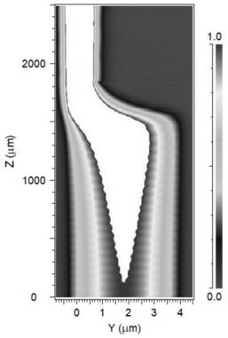
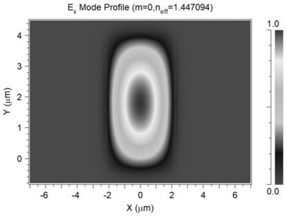
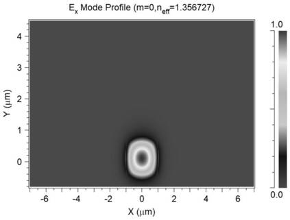
[0032] An embodiment of the present invention provides a speckle converter based on an arrayed waveguide grating and a waveguide detector, which adopts a double-step waveguide structure including a first waveguide and a second waveguide, both of which are opposite The tapered waveguide structure has a parabolic transition mode; the large end face of the first waveguide is aligned with the large end face of the second waveguide, the large end face of the first wavegu...


PUM

PropertyMeasurementUnit
refractive indexaaaaaaaaaa

Abstract

The spot size converter based on the arrayed waveguide grating and the waveguide type detector adopts a double-step type waveguide structure comprising a first waveguide and a second waveguide, the first waveguide and the second waveguide are both of reverse conical waveguide structures, and the transition mode of the first waveguide and the second waveguide is parabola type transition; the large end face of the first waveguide is aligned with the large end face of the second waveguide, the large end face of the first waveguide is an incident face of output light of the array waveguide grating, the small end face of the second waveguide is a light emitting face, and light originally limited in a core layer of the first waveguide is coupled into a core layer of the second waveguide, so that a mode field is reduced, and the light emitting efficiency is improved. A mode field in the array waveguide grating is converted into a mode field in the ridge waveguide of the waveguide type detector, and matching of the array waveguide grating and the mode field of the waveguide type detector is achieved. The end face coupling mode is adopted, the light field is coupled into the absorption area from the side face, loss and scattering of the light field in the waveguide propagation process are reduced, the light coupling efficiency is further improved, and integrated application of the photoelectric detector is facilitated.

Description

technical field [0001] The invention relates to the technical field of silicon-based optical integrated chips, in particular to a mode speckle converter based on an arrayed waveguide grating and a waveguide detector. Background technique [0002] In recent years, photonic integrated circuits are developing in the direction of small size and high density. Devices produced by planar optical waveguide technology have the advantages of small size, low loss, high integration, and easy scale production, and are widely used in optical communication systems. This technology is a technology in which an optical waveguide is fabricated in a planar substrate and optical signals are transmitted in the waveguide. Realizing the optical coupling of Arrayed Waveguide Grating (AWG) to the waveguide detector is the key to the integration of optical devices from the laboratory to the practical. The coupling efficiency directly affects the performance of various integrated optical products. ...

Claims


Application Information

Patent Timeline
Patent Type & Authority Applications(China)
IPC IPC(8): G02B6/122G02B6/12
CPCG02B6/1228G02B6/12002G02B6/12004
Inventor 陈远祥付佳孙尚斌朱虎孙莉萍李欣国林尚静余建国王亮蒋忠君何伟江致远
Owner BEIJING UNIV OF POSTS & TELECOMM
Why Eureka
Try Eureka