Slit-embedded one-dimensional photonic crystal nano-beam cavity biosensor

A technology of dimensional photonic crystal and biosensor, applied in the field of photonic crystal sensor, can solve the problems of small overlapping volume between biological target and optical field, large absorption loss of biosensor, low robustness of manufacturing process error, etc., and achieves improvement of refractive index. Effects of sensitivity, lower limit of refractive index detection, and high robustness

Pending Publication Date: 2022-04-26
SHANGHAI INST OF MICROSYSTEM & INFORMATION TECH CHINESE ACAD OF SCI
View PDF0 Cites 0 Cited by
  • Summary
  • Abstract
  • Description
  • Claims
  • Application Information

AI Technical Summary

Problems solved by technology

[0004] Problems existing in the existing one-dimensional photonic crystal nano-beam cavity biosensor: 1. The dielectric mode one-dimensional photonic crystal nano-beam cavity works in the C band of the communication band, resulting in excessive absorption loss and Q value (quality factor) of the biosensor working in aqueous solution. ) attenuation is obvious; 2. In the dielectric mode one-dimensional photonic crystal nanobeam cavity, the light field is mainly localized in the high refractive index region to obtain a high quality factor, resulting in a small overlapping volume between the biological target and the light field, and poor refractive index sensitivity. High problem; 3. High-quality factor dielectric mode one-dimensional photonic crystal nanobeam cavity test requires high-resolution optical test system, and the robustness of manufacturing process error is low

Method used


Image

  • Slit-embedded one-dimensional photonic crystal nano-beam cavity biosensor
  • Slit-embedded one-dimensional photonic crystal nano-beam cavity biosensor
  • Slit-embedded one-dimensional photonic crystal nano-beam cavity biosensor

Examples


Embodiment Construction

[0025] The present invention is further elaborated below in conjunction with specific embodiments. It should be understood that these embodiments are used only to illustrate the present invention and not to limit the scope of the present invention. Further it should be understood that, after reading the contents of the present invention, those skilled in the art may make various modifications or modifications to the present invention, these equivalent forms also fall within the scope of the claims attached to the present application.

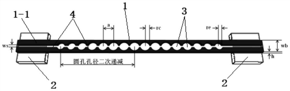
[0026] Embodiments of the present invention relates to a one-dimensional photonic crystal nano-beam cavity biosensor embedded in a slit, see Figure 1 , including silicon waveguide 1 and nano-beam cavities, which are located on silicon waveguide 1. The structure of the nanobead cavity is: etching a column of through holes 3 on the center symmetry of silicon waveguide 1 and embedded in slit 4. The through hole 3 of the present embodiment is a circula...


PUM

PropertyMeasurementUnit
widthaaaaaaaaaa
widthaaaaaaaaaa
thicknessaaaaaaaaaa

Abstract

The invention relates to a slit-embedded one-dimensional photonic crystal nano-beam cavity biosensor. The slit-embedded one-dimensional photonic crystal nano-beam cavity biosensor comprises a silicon waveguide; the nanometer beam cavity is positioned on the silicon waveguide; a plurality of through holes are etched in the nanometer beam cavity, the plurality of through holes are symmetrical about the center of the silicon waveguide, a slit is formed in the plurality of through holes, and the slit penetrates through the plurality of through holes. According to the invention, the low-concentration detection lower limit of the cancer early marker microRNA can be obtained.

Description

Technical field [0001] The present invention relates to the field of photonic crystal sensor technology, in particular to a one-dimensional photonic crystal nanobeadminal cavity biosensor embedded in a slit. Background [0002] Cancer has become the leading cause of death in noncommunicable diseases worldwide, and the lower limit of detection of microRNAs, a marker of early cancer, can improve cancer five-year survival and reduce cancer mortality. Photonic crystal sensing technology can use the label-free surface modification reaction to achieve the lower limit detection of microRNAs at low concentrations, and has the advantages of strong anti-interference ability and easy integration, which has gradually become a hot topic in the field of biomedical sensing. [0003] At present, the sensing research on the nano-beam cavity of one-dimensional photonic crystals is mainly used for gas sensing, focusing on the optimization of quality factors, and the research on the lower limit of ...

Claims


Application Information

Patent Timeline
Patent Type & Authority Applications(China)
IPC IPC(8): G01N21/41G02B6/122
CPCG01N21/41G02B6/1225G02B2006/12138
Inventor 史清梁丽娟赵建龙
Owner SHANGHAI INST OF MICROSYSTEM & INFORMATION TECH CHINESE ACAD OF SCI
Why Eureka
Try Eureka