GPP diode chip production process adopting honeycomb photomask and knife scraping method
A production process, honeycomb-shaped technology, applied in the field of GPP diode chip production process, can solve problems such as graphic structure obstruction, achieve the effect of reducing environmental protection pressure, reducing costs, and saving consumables
- Summary
- Abstract
- Description
- Claims
- Application Information
AI Technical Summary
Problems solved by technology
Method used
Image

Examples
Embodiment 1
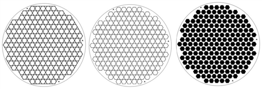
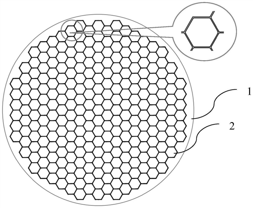
[0047] In this embodiment, a kind of GPP diode chip production process using honeycomb photolithography plate and knife scraping method is provided. A hexagonal honeycomb double-groove photolithography mask suitable for negative glue is used in this production process. The stencil, this hexagonal honeycomb double-groove lithography mask, includes a first mask and a second mask, wherein the first mask is used for the first exposure, and the second mask The plate is used for exposure during the second overlay. The photolithography mask plate can be applied in the knife-scraping process of GPP glass packaging, and only one exposure machine is needed to complete the first exposure and the second overlay exposure to realize overlay.
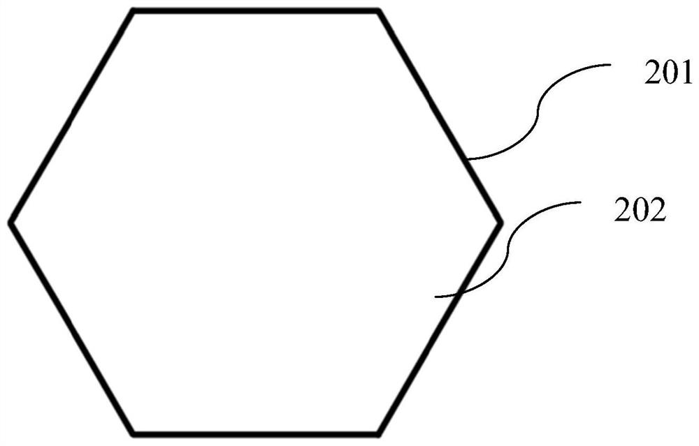
[0048] In order to facilitate the understanding of the flow of the subsequent GPP diode chip production process of the present invention, the specific structures of the first mask and the second mask in the hexagonal honeycomb double-groove photolitho...
Embodiment 2
[0092] In this embodiment, a GPP diode chip production process using a honeycomb photolithography plate and a knife scraping method is provided. The difference between this process and Example 1 is that it is suitable for positive resist, so the hexagonal honeycomb it uses The double-groove photolithographic mask should also be matched with the positive resist.
[0093] Specifically, in this embodiment, the structures of the first mask and the second mask are basically the same as in Embodiment 1, and the only difference is that the first photolithographic mask layer 2 and the second photolithographic mask layer The light transmission types of the light-transmitting area and the light-impermeable area in 4 are just opposite to those in the embodiment, that is to say, the light-transmitting areas in the two photolithographic mask layers in the embodiment 1 are both is an opaque area, while the opaque area in the two photolithography mask layers in Embodiment 1 is a light-transm...
PUM
| Property | Measurement | Unit |
|---|---|---|
| Thickness | aaaaa | aaaaa |
Abstract
Description
Claims
Application Information