Double-spectrum film type multi-junction photovoltaic device structure

A photovoltaic device and thin-film technology, which is applied in the field of dual-spectrum thin-film multi-junction photovoltaic device structure, can solve problems such as unsatisfactory use requirements and performance degradation, and achieve the effects of improving photoelectric conversion efficiency, reducing thickness, and improving efficiency

Active Publication Date: 2022-04-29
上海镓芯科技有限公司
View PDF5 Cites 0 Cited by
  • Summary
  • Abstract
  • Description
  • Claims
  • Application Information

AI Technical Summary

Problems solved by technology

Conventional multi-junction solar cells are designed in strict accordance with the spectral structure of the sun. Under various human light source conditions, due to the mismatch of the spectrum, the performance will be greatly reduced and cannot meet the needs of use.

Method used


Image

  • Double-spectrum film type multi-junction photovoltaic device structure
  • Double-spectrum film type multi-junction photovoltaic device structure
  • Double-spectrum film type multi-junction photovoltaic device structure

Examples


Embodiment Construction

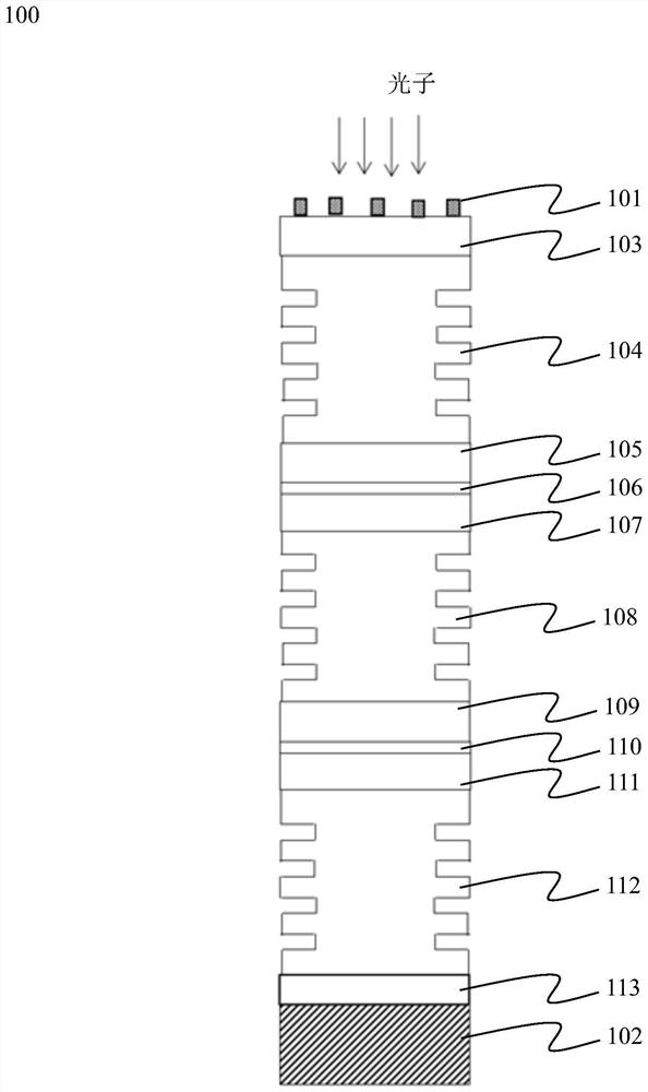
[0035] The following examples are intended to better understand the essence of the present invention, without limiting the invention to the described examples. In addition, the terms "first" and "second" are used for distinguishing descriptions, and should not be understood as indicating or implying relative importance. In the description of the embodiments, concepts such as the upper surface of the semiconductor thin film layer and the lower surface of the semiconductor thin film layer are used. It should be understood that the "upper" and "lower" mentioned here are relative to the direction of photon incidence, that is, "upper" refers to the side close to the photon incidence direction, and "down" refers to the side away from the photon incidence direction. side.

[0036] Those skilled in the art can understand that the beneficial effects of the present invention can still be obtained by making changes to these embodiments without departing from the principle of the present...


PUM

PropertyMeasurementUnit
thicknessaaaaaaaaaa
thicknessaaaaaaaaaa
thicknessaaaaaaaaaa

Abstract

The invention relates to a double-spectrum thin film type multi-junction photovoltaic device structure which is named as a double-spectrum quantum well cascade composite junction. The structure comprises three PN junctions with a multi-quantum well structure, and the three PN junctions respectively form absorption junctions; a tunnel junction is arranged between the absorption junctions, so that the two adjacent absorption junctions are electrically communicated to form a free carrier path; in addition, by means of energy band engineering design, the electron-hole energy level difference of the absorption junction located in the middle is larger than that of the absorption junctions on the two sides. The structure can greatly improve the quantum efficiency of internal photoelectric conversion, can adapt to multispectral incident light, including solar spectrum and various human illumination light sources, such as LED lamps, incandescent lamps, halogen lamps and fluorescent lamps, can automatically realize current matching among multi-junction batteries under the spectrum conditions of various light sources, and can automatically realize current matching among the multi-junction batteries when different light sources are switched. And high photoelectric conversion efficiency is dynamically realized.

Description

technical field [0001] The invention relates to a dual-spectrum thin-film multi-junction photovoltaic device structure in the field of semiconductors; the photovoltaic device with the structure can adapt to various spectral conditions. Background technique [0002] Photoelectric effect is the basic theory of photovoltaic industry development. Since 1887, when the German physicist Hertz was studying the properties of electromagnetic waves, he accidentally discovered the phenomenon that electrons on the metal surface would overflow from the metal surface under the influence of light, announcing the photoelectric effect to the world. More than 100 years have passed, and with the increasing demand for clean energy, photovoltaic power generation, which generates electricity from light energy, has become the focus of industry applications. [0003] At present, the development of semiconductor materials has further promoted photovoltaic power generation technology. The prior art ...

Claims


Application Information

Patent Timeline
Patent Type & Authority Applications(China)
IPC IPC(8): H01L31/0224H01L31/0392H01L31/052H01L31/06H01L31/0687
CPCH01L31/022425H01L31/0392H01L31/052H01L31/06H01L31/0687Y02E10/544
Inventor 王伟明
Owner 上海镓芯科技有限公司
Why Eureka
Try Eureka