SOI wafer with asymmetric silicon nanoparticle array structure and preparation method thereof

A silicon nanoparticle and nanoparticle technology, applied in the field of optical devices, can solve the problems of low integration efficiency, complex processing technology of superstructure functional units, high preparation cost, etc., to achieve enhanced local field strength, enhanced nonlinear effect, and easy The effect of processing

Pending Publication Date: 2022-05-13
TSINGHUA UNIV
View PDF0 Cites 0 Cited by
  • Summary
  • Abstract
  • Description
  • Claims
  • Application Information

AI Technical Summary

Problems solved by technology

However, the processing technology of split resonator rings and L-shaped, triangular and other superstructural functional units is too complex, and when applied to integrated nanoparticle array structures, the integration efficiency is low and the preparation cost is high.

Method used


Image

  • SOI wafer with asymmetric silicon nanoparticle array structure and preparation method thereof
  • SOI wafer with asymmetric silicon nanoparticle array structure and preparation method thereof
  • SOI wafer with asymmetric silicon nanoparticle array structure and preparation method thereof

Examples


Embodiment Construction

[0032] The following will clearly and completely describe the technical solutions in the embodiments of the present invention with reference to the accompanying drawings in the embodiments of the present invention. Obviously, the described embodiments are only some, not all, embodiments of the present invention. Based on the embodiments of the present invention, all other embodiments obtained by persons of ordinary skill in the art without making creative efforts belong to the protection scope of the present invention.

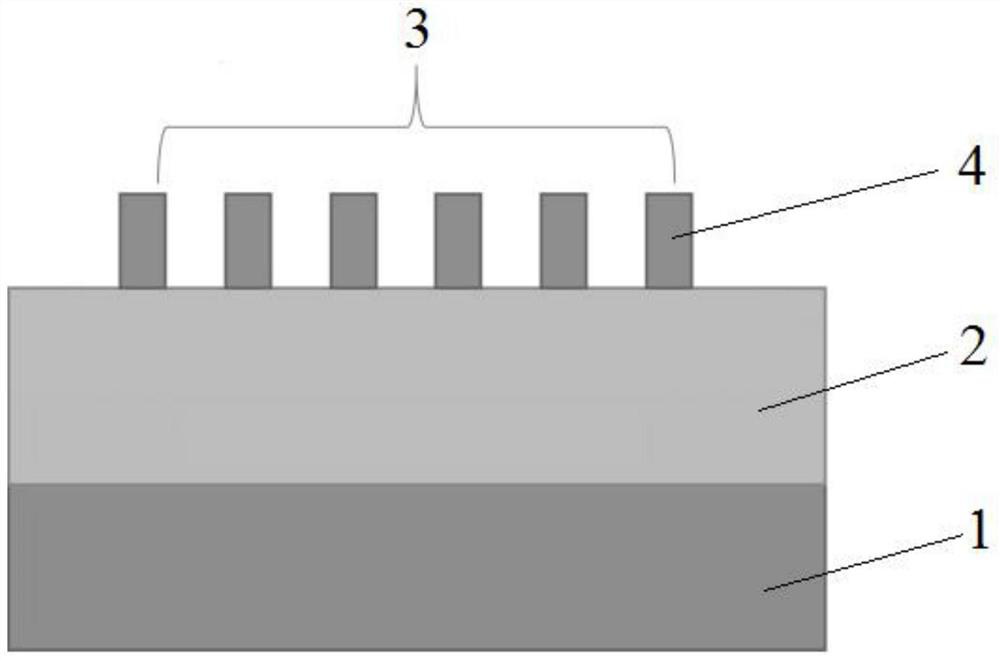
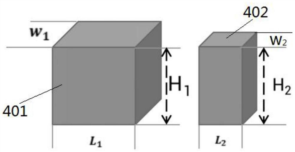
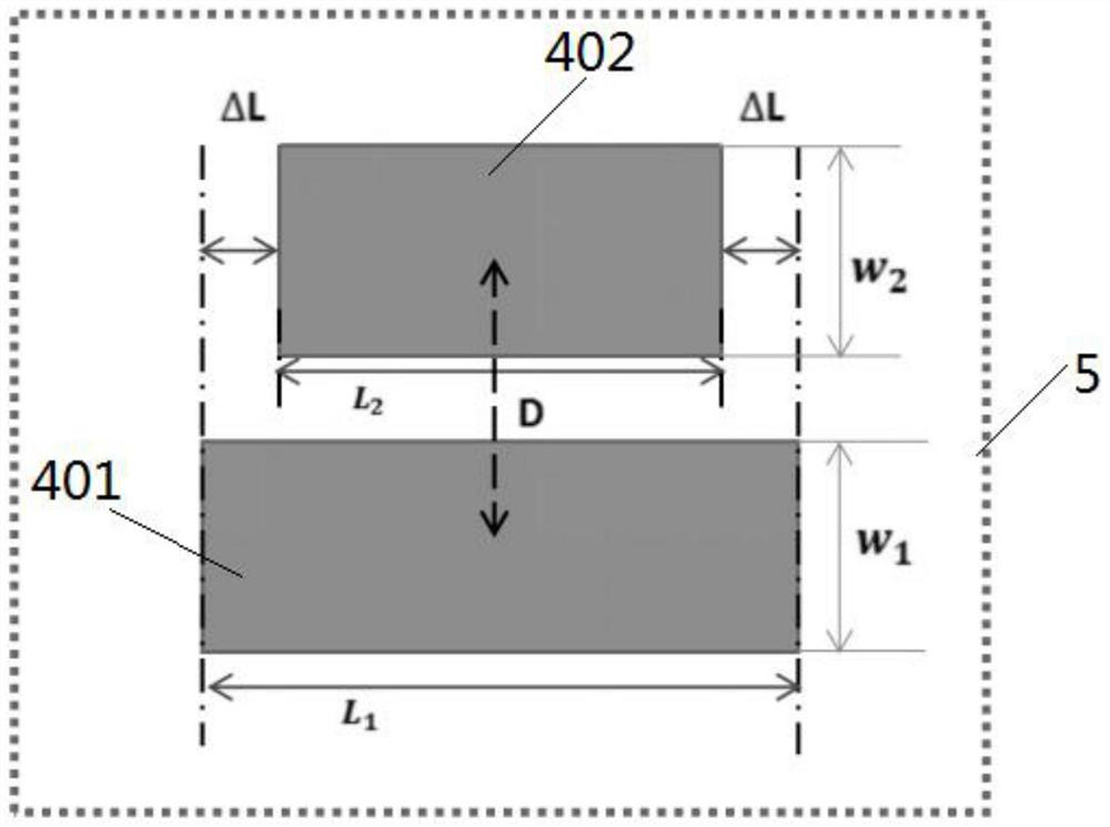
[0033] The object of the present invention is to provide an SOI wafer with an asymmetric silicon nanoparticle array structure and a preparation method, so as to enhance the nonlinear effect of the silicon nanoparticle array structure and simplify the processing technology.

[0034] In order to make the above objects, features and advantages of the present invention more comprehensible, the present invention will be further described in detail below in conjuncti...


PUM

PropertyMeasurementUnit
refractive indexaaaaaaaaaa

Abstract

The invention relates to an SOI (Silicon On Insulator) wafer with an asymmetric silicon nanoparticle array structure and a preparation method. The SOI wafer comprises a silicon substrate layer, a silicon dioxide buried layer and a silicon nanoparticle array, the nano-particle array is formed by periodically arranging an even number of elements; each element comprises two cuboid nano-particles with different sizes, and the two cuboid nano-particles are arranged in parallel or in a straight line; in the parallel or linear arrangement mode, the first cuboid nano-particles are located on one side of the second cuboid nano-particles; taking a connecting line between the central point of the first cuboid nanoparticle and the central point of the second cuboid nanoparticle as a symmetric axis; and the first cuboid nano-particles and the second cuboid nano-particles are respectively arranged in an axial symmetry manner relative to the symmetry axis. The asymmetric structure adopted by the silicon nanoparticle array enhances the local field intensity of optical signals, the nonlinear combination with the silicon material further enhances the nonlinear effect of the silicon nanoparticle array, and the processing technology is simplified.

Description

technical field [0001] The invention relates to the technical field of optical devices, in particular to an SOI wafer with an asymmetric silicon nanoparticle array structure and a preparation method thereof. Background technique [0002] The nonlinear effect originates from the interaction between the light and the waveguide, that is, the resonance between the electric field of the optical signal and the outer electrons of the atoms generates nonlinear polarization. Metals, such as gold (Au), silver (Ag), and copper (Cu) nano-metal particle arrays, highly localize the light field energy on the metal surface and can exhibit nonlinear effects. [0003] Compared with the above-mentioned metal materials, the Raman gain coefficient of silicon is 3000 times that of quartz materials and depends on the polarization characteristics. The wavelength range is within the transparent range of less than 2.2 μm, and it shows obvious nonlinear optical characteristics. The nonlinear refractiv...

Claims


Application Information

Patent Timeline
Patent Type & Authority Applications(China)
IPC IPC(8): B81B1/00B81C1/00
CPCB81B1/00B81C1/00031B81C1/00523
Inventor 张小平张梦雨王逸松李铭晖
Owner TSINGHUA UNIV
Why Eureka
Try Eureka