Hyperspectral system based on MEMS and spectrometer
A technology of hyperspectral and spectroscopic systems, applied in spectrometry/spectrophotometry/monochromator, instruments, scientific instruments, etc., can solve the problem of inability to collect spectral information at one time, unable to image multiple points at one time, and low energy sensitivity and other problems, to achieve the effect of improving the spectral wavelength range, small size and high resolution
- Summary
- Abstract
- Description
- Claims
- Application Information
AI Technical Summary
Problems solved by technology
Method used
Image
Examples
Embodiment 1
[0036] The spectral imaging device is used to obtain almost continuous spectral data of each pixel while obtaining a large number of narrow-band continuous spectral images of ground objects. Spectral imaging devices are divided into multispectral imaging devices, hyperspectral imaging devices, and hyperspectral imaging devices according to the spectral resolution of the sensor. The spectral resolution of the multi-spectral imaging device is on the order of delta_lambda / lambda=0.1, and there are generally only a few bands in the visible and near-infrared regions. The spectral resolution of the hyperspectral imaging device is on the order of delta_lambda / lambda=0.01, and there are tens to hundreds of bands in the visible and near-infrared regions, and the spectral resolution can reach the nm level. The spectral resolution of the hyperspectral imaging device is on the order of delta_lambda / lambda=0.001, and can reach thousands of wavebands in the visible and near-infrared regions...
Embodiment 2
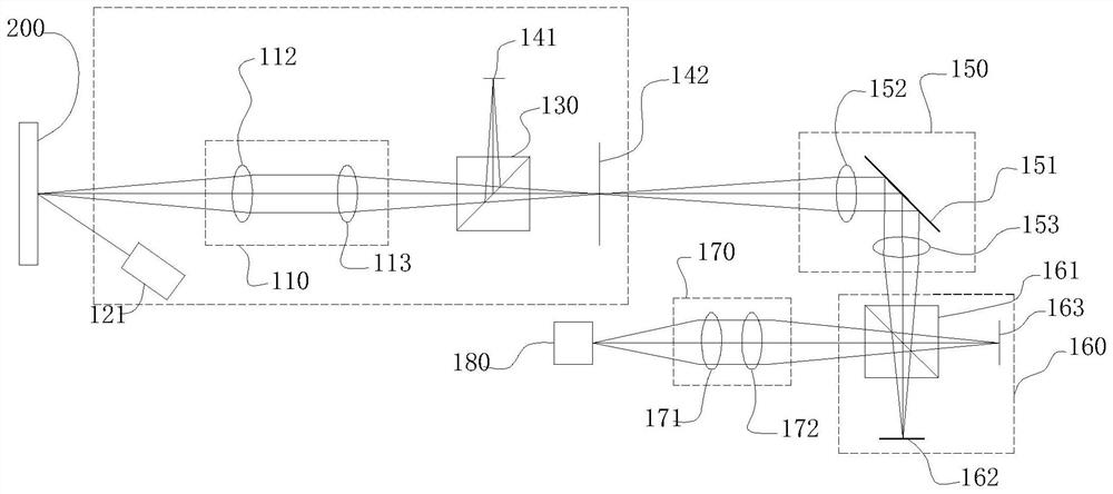
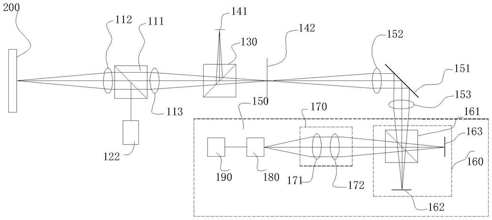
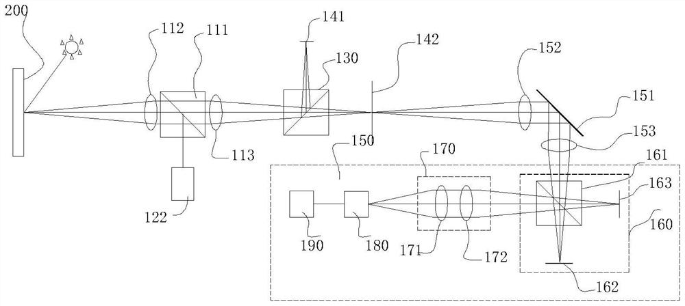
[0040] In order to solve the above-mentioned problems, the application also provides a hyperspectral system based on MEMS, including a light source and a beam processing unit, and it also includes an interference system 160. The interference system 160 includes a MEMS translation micromirror 163, and the light source is processed by the beam processing unit The light beam 142 enters the MEMS translational micromirror 163 , and the MEMS translational micromirror 163 modulates and reflects the light beam 142 .
Embodiment 3
[0042] On the basis of Embodiment 2, the interference system 160 of this embodiment also includes a third beam splitting system 161 and a plane fixed mirror 162; the light beam 142 is divided into two beams of light through the third beam splitting system 161, one beam enters the plane fixed mirror 162, and passes through the plane mirror 162. The plane fixed mirror 162 returns to the third beam splitting system 161 , and the other beam enters the MEMS translational micromirror 163 and returns to the third beam splitting system 161 through the MEMS translational micromirror 163 .
[0043] This embodiment also includes that the micromirror unit 150 includes a first lens 152 and a second lens 153; the light beam 142 is used as the input of the micromirror unit 150, and is transmitted to the MEMS scanning micromirror 151 by the first lens 152, and then reflected by the second lens 153 output. The light beams 142 transmitted by the first lens 152 are read one by one by rotating th...
PUM
 Abstract
Description
Claims
Application Information
 - R&D
- Intellectual Property
- Life Sciences
- Materials
- Tech Scout
- Unparalleled Data Quality
- Higher Quality Content
- 60% Fewer Hallucinations
Browse by: Latest US Patents, China's latest patents, Technical Efficacy Thesaurus, Application Domain, Technology Topic, Popular Technical Reports.
© 2025 PatSnap. All rights reserved.Legal|Privacy policy|Modern Slavery Act Transparency Statement|Sitemap|About US| Contact US: help@patsnap.com


