Preparation method of low-defect silicon carbide epitaxial material

A technology of epitaxial materials and silicon carbide, which is applied in semiconductor/solid-state device manufacturing, electrical components, circuits, etc., can solve problems that restrict device performance, achieve low surface defect density, uniform temperature field, and reduce inhomogeneity

Pending Publication Date: 2022-05-13
ZHEJIANG UNIV HANGZHOU GLOBAL SCI & TECH INNOVATION CENT
View PDF0 Cites 0 Cited by
  • Summary
  • Abstract
  • Description
  • Claims
  • Application Information

AI Technical Summary

Problems solved by technology

However, various types of defects still inevitably exist in the prepared silicon carbide film, and these defects will restrict the performance of devices fabricated on the film.

Method used


Image

  • Preparation method of low-defect silicon carbide epitaxial material
  • Preparation method of low-defect silicon carbide epitaxial material

Examples


Embodiment Construction

[0021] In order to facilitate the understanding of those skilled in the art, the present invention will be further described in detail below in conjunction with specific embodiments.

[0022] Embodiments of the present invention firstly provide a method for preparing a low-defect silicon carbide epitaxial material.

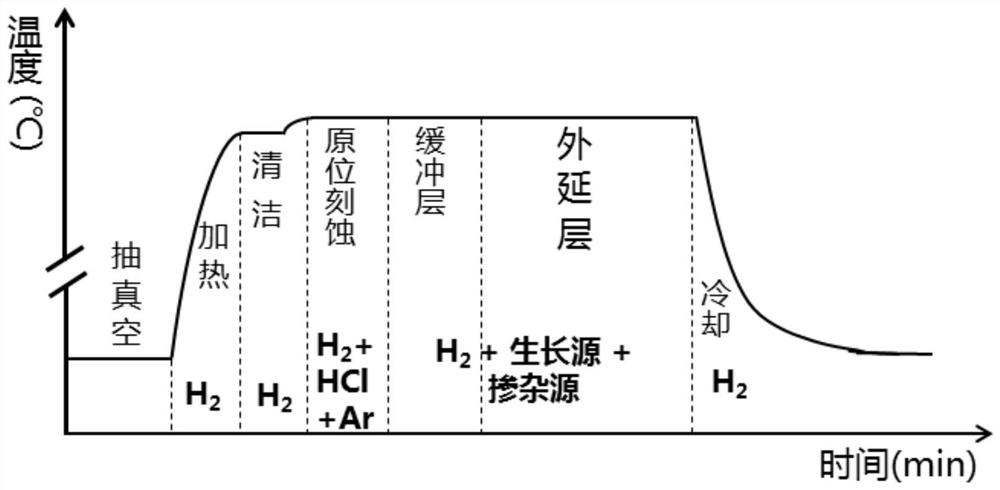
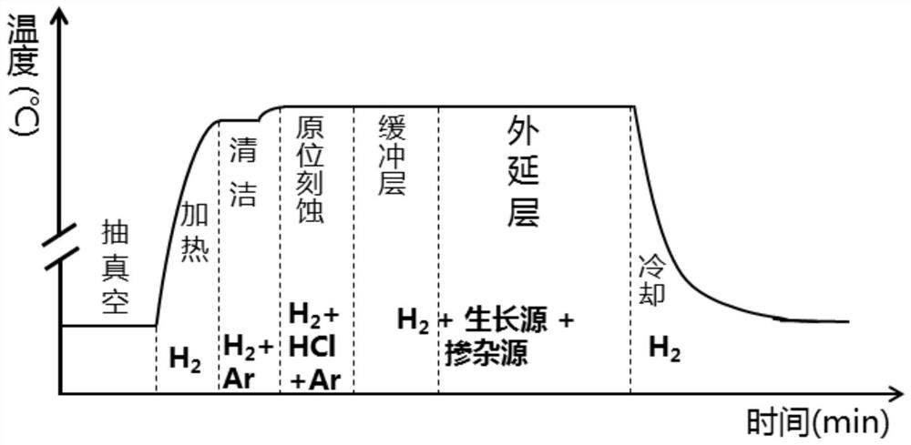
[0023] Please refer to figure 1 , is a schematic diagram of a method for preparing a low-defect silicon carbide epitaxial material provided by the first embodiment of the present invention.

[0024] The first stage is the preparatory work before preparation, which specifically includes: transferring the cleaned silicon carbide off-axis substrate to the graphite disk base in the CVD equipment, and the CVD equipment is vacuumed. In this embodiment, the silicon carbide off-axis substrate is a 4H-SiC or 6H-SiC substrate that is biased to the silicon surface of the direction by 0.2-8° (0001), and the CVD equipment adopts hot-wall CVD equipment, in other embodiments,...


PUM


Abstract

The invention provides a preparation method of a low-defect silicon carbide epitaxial material, which relates to the technical field of silicon carbide epitaxial materials, and comprises the following steps: introducing argon and mixed gas consisting of hydrogen chloride and hydrogen into a reaction chamber to carry out in-situ etching on a silicon carbide off-axis substrate for 5-20 minutes. The introduction of hydrogen chloride and hydrogen enables a Si component and a C component on the surface of the silicon carbide off-axis substrate to reach similar removal speeds, so that a smoother substrate surface is obtained, the introduction of argon enables a temperature field in the reaction chamber to be more uniform, anisotropy generated when the silicon carbide off-axis substrate is etched by hydrogen chloride and hydrogen in the reaction chamber is reduced, and the yield of the silicon carbide off-axis substrate is improved. The non-uniformity of surface etching and the surface defects of the substrate extending to the epitaxial layer are reduced, and the silicon carbide epitaxial material obtained through the growth of the buffer layer and the growth of the epitaxial layer has the advantages of low surface defect density and high uniformity.

Description

technical field [0001] The invention relates to the technical field of silicon carbide epitaxial materials, in particular to a method for preparing low-defect silicon carbide epitaxial materials. Background technique [0002] In recent years, silicon carbide substrates, epitaxial materials and devices are growing steadily and rapidly, and in some fields it is gradually replacing traditional silicon and gallium arsenide materials. Silicon carbide has better material properties than silicon and gallium arsenide. At present, silicon carbide power electronic devices have been widely used in hybrid electric vehicles, electric vehicle equipment, silicon carbide device power modules, silicon carbide inverter air conditioners, silicon carbide inverters and other fields. Compared with traditional silicon devices, the biggest advantage of silicon carbide power electronic devices is that they can work at high voltage and ultra-high voltage. In order to realize the development of silic...

Claims


Application Information

Patent Timeline
Patent Type & Authority Applications(China)
IPC IPC(8): H01L21/02
CPCH01L21/02661H01L21/02378H01L21/02529H01L21/0262
Inventor 刘小平王蓉皮孝东李佳君杨德仁
Owner ZHEJIANG UNIV HANGZHOU GLOBAL SCI & TECH INNOVATION CENT
Why Eureka
Try Eureka