Lateral light mode control high-power semiconductor device and preparation method thereof

A semiconductor, high-power technology, used in semiconductor devices, electrical components, circuits, etc., can solve the problems of high beam quality, high brightness, and high integration, and achieve the effect of improving light output brightness, reducing divergence angle, and increasing thermal conductivity.

Active Publication Date: 2022-07-05
SUZHOU EVERBRIGHT PHOTONICS CO LTD +1
View PDF0 Cites 0 Cited by
  • Summary
  • Abstract
  • Description
  • Claims
  • Application Information

AI Technical Summary

Problems solved by technology

[0004] Therefore, the technical problem to be solved by the present invention is to overcome the problems of high light output brightness, high beam quality, low cost, and high integration in the prior art, so as to provide a side light mode control high-power semiconductor device and its preparation method

Method used


Image

  • Lateral light mode control high-power semiconductor device and preparation method thereof
  • Lateral light mode control high-power semiconductor device and preparation method thereof
  • Lateral light mode control high-power semiconductor device and preparation method thereof

Examples


Embodiment 1

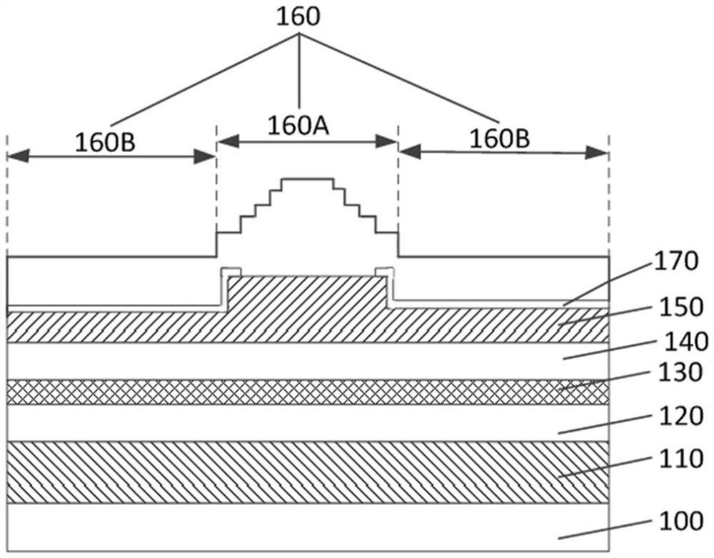
[0044] An embodiment of the present invention provides a lateral light mode control high-power semiconductor device, refer to figure 1 ,include:

[0045] semiconductor substrate layer 100;

[0046] an active layer 130 located on the semiconductor substrate layer 100;

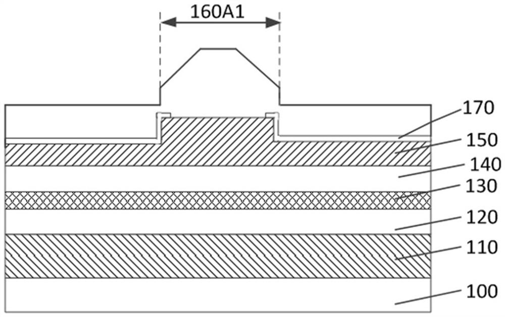
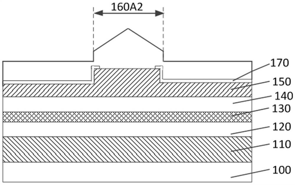
[0047] The front electrode layer 160 located on the side of the active layer 130 away from the semiconductor substrate layer 100, the front electrode layer 160 includes an electrode injection region 160A; it is self-directed in the slow axis direction of the lateral light mode control high-power semiconductor device. The thickness of the electrode implantation region 160A decreases gradually from the central region of the electrode implantation region 160A to the edge region of the electrode implantation region 160A.

[0048] In this embodiment, the lateral light mode control high-power semiconductor device is an edge-emitting semiconductor laser.

[0049] The material of the semiconductor substrate layer 100...

Embodiment 2

[0075] The difference between this embodiment and Embodiment 1 is that: refer to Image 6 , the lateral light mode control high-power semiconductor device further includes: a thermal compensation layer 210, the thermal compensation layer 210 is located on the side of the non-injection electrode region 160B facing the active layer 130 and in contact with the non-injection electrode region 160B, the thermal compensation layer 210 The thermal conductivity of is less than that of the solder layer.

[0076] In this embodiment, since the thermal conductivity of the thermal compensation layer 210 is smaller than that of the soldering layer, the thermal conductivity of the thermal compensation layer 210 is small, which reduces the impact of the semiconductor film directly under the thermal compensation layer 210 on non-implantation The thermal conductivity of the electrode region 160B reduces the temperature gradient of the active layer 130 directly under the thermal compensation laye...

Embodiment 3

[0090] The difference between this embodiment and Embodiment 2 is: refer to Figure 7 , the thermal compensation layer 210a includes a first compensation region M1 and a second compensation region M2 arranged in the slow axis direction, and the distance from the first compensation region M1 to the electrode injection region 160A is smaller than the second compensation region M2 The distance to the electrode implantation region 160A; the thickness of the second compensation region M2 is greater than the thickness of the first compensation region M1.

[0091] against Figure 7 Thermal compensation layer, the simulation diagram of the effect is as follows Figure 8 ,and Figure 7 The structure also compares figure 1 and Image 6 By increasing the thickness of the second compensation region M2, the temperature of the active layer under the first compensation region M1 adjacent to the ridge region is further increased, and the temperature of the active layer under the first com...


PUM

PropertyMeasurementUnit
thicknessaaaaaaaaaa
thicknessaaaaaaaaaa
thicknessaaaaaaaaaa

Abstract

A lateral light mode control high-power semiconductor device, a preparation method thereof, and a semiconductor packaging structure, the lateral light mode control high-power semiconductor device comprises: a semiconductor substrate layer; an active layer located on the semiconductor substrate layer; A front electrode layer on the side of the active layer away from the semiconductor substrate layer, the front electrode layer includes an electrode injection region; from the central region of the electrode injection region to the electrode in the slow axis direction of the lateral light mode control high-power semiconductor device In the edge region of the implanted region, the thickness of the electrode implanted region decreases. The semiconductor device has the advantages of high brightness, high beam quality, low cost, and high integration.

Description

technical field [0001] The invention relates to the technical field of semiconductors, in particular to a lateral light mode control high-power semiconductor device and a preparation method thereof. Background technique [0002] The semiconductor light-emitting structure is a device that produces stimulated emission with a certain semiconductor material as a working substance. Its working principle is: through a certain excitation method, between the energy band (conduction band and valence band) of the semiconductor material, or the Between the energy band of the material and the energy level of the impurity (acceptor or donor), the population inversion of non-equilibrium carriers is realized. When a large number of electrons and holes in the state of population inversion recombine, stimulated emission occurs. Because of its small size and high electro-optical conversion efficiency, semiconductor light-emitting devices are widely used. [0003] In the prior art, high-power...

Claims


Application Information

Patent Timeline
Patent Type & Authority Patents(China)
IPC IPC(8): H01L33/38H01L33/64H01L33/00
CPCH01L33/38H01L33/642H01L33/641H01L33/005H01L2933/0016
Inventor 王俊刘武灵谭少阳王邦国赵武廖新胜
Owner SUZHOU EVERBRIGHT PHOTONICS CO LTD
Why Eureka
Try Eureka