Supercharge Your Innovation With Domain-Expert AI Agents!

Light emitting diode, light emitting diode package, and plant lighting device

A technology of light-emitting diodes and semiconductors, applied in the fields of botanical equipment and methods, semiconductor devices, energy-saving measures, etc., can solve the problems of consumption or absorption, and light less than the critical angle may be emitted during one or more oscillations. , to achieve the effect of improving luminous brightness and improving light extraction efficiency

Pending Publication Date: 2022-05-13
TIANJIN SANAN OPTOELECTRONICS
View PDF5 Cites 0 Cited by
  • Summary
  • Abstract
  • Description
  • Claims
  • Application Information

AI Technical Summary

Problems solved by technology

In the prior art, the ODR total reflection structure fully reflects the light greater than the critical angle back to the inside of the semiconductor epitaxial stack and emerges from the light-emitting surface, and the light less than the critical angle may be emitted or consumed during one or more oscillations. or absorb

Method used


Image

  • Light emitting diode, light emitting diode package, and plant lighting device
  • Light emitting diode, light emitting diode package, and plant lighting device
  • Light emitting diode, light emitting diode package, and plant lighting device

Examples


Embodiment 1

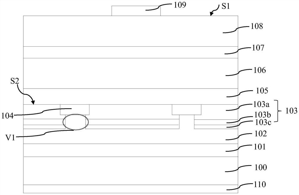
[0029] This embodiment provides the following light emitting diode, such as figure 1 The cross-sectional schematic diagram shown, which includes the following stacked layers: 100: substrate; 101: metal bonding layer; 102: reflective layer; 103: light-transmitting dielectric layer structure; 103a: first sublayer; 103b: second sublayer ; 103c: third sublayer; 104: ohmic contact layer; 105: current spreading layer; 106: second conductivity type semiconductor layer; 107: active layer; 108: first conductivity type semiconductor layer; 109: first electrode; 110: second electrode.

[0030] In this embodiment, the light-emitting diode has a semiconductor epitaxial stack, which is obtained by MOCVD or other growth methods, and is a semiconductor material that can provide conventional radiation such as ultraviolet, blue, green, yellow, red, and infrared light. Specifically, it can be 200~950nm materials, such as common nitrides, such as gallium nitride-based semiconductor epitaxial sta...

Embodiment 2

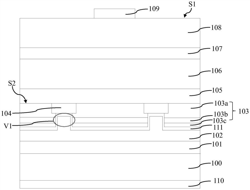
[0046] and Example 1 figure 1 Compared with the light emitting diode shown, in order to improve the adhesion between the semiconductor epitaxial stack and the reflective layer 102, as figure 2 As shown, the light emitting diode also includes an adhesive layer 111, the adhesive layer 111 is formed on the side of the light-transmitting dielectric layer structure 103 away from the semiconductor epitaxial stack, the adhesion layer 111 is a light-transmitting conductive material, The light-transmitting conductive material is specifically IZO or ITO, etc., and is more preferably a material with good adhesion between the light-transmitting dielectric layer structure 103 and the reflective layer 102, such as gold or silver.

[0047] The thickness of the adhesion layer is greater than 2nm, preferably the thickness of the adhesion layer is more than 5nm, so as to achieve a better adhesion effect. In some optional embodiments, the adhesive layer is a continuous film layer, and in some ...

Embodiment 3

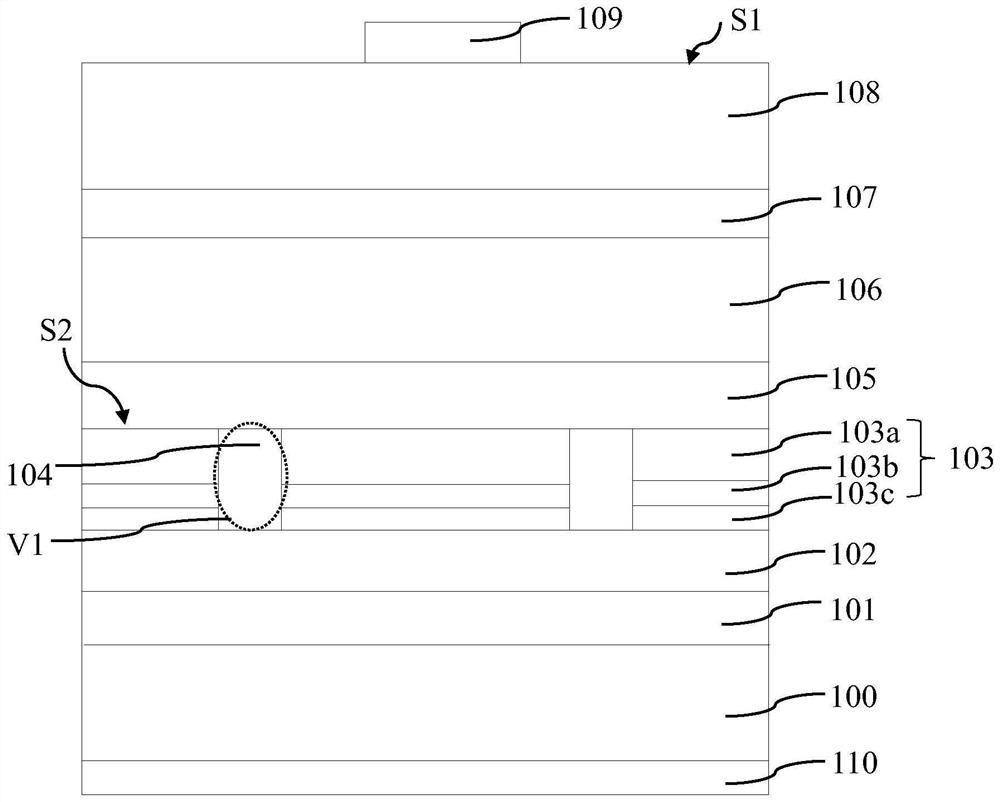
[0049] image 3 It is a schematic structural diagram of a light emitting diode in another embodiment of the present invention. Such as image 3 As shown, the light-transmitting dielectric layer structure 103 has a through hole V1, the ohmic contact layer 104 is disposed in at least one through-hole V1 of the light-transmitting dielectric layer structure 103, and the ohmic contact layer 104 passes through the through-hole V1. The hole V1 forms an ohmic contact with the current spreading layer 105, and the current is evenly transmitted from the metal bonding layer 101, the through hole V1 connecting the reflective layer 102 and the ohmic contact layer 104 to the semiconductor epitaxial stack, so the ohmic contact layer 104 covers at least a plurality of The area of ​​the via hole V1 does not completely cover one side of the contact current spreading layer 105 . The ohmic contact layer 104 uses a conductive metal or a transparent conductive layer. The conductive metal is prefe...


PUM

PropertyMeasurementUnit
Thicknessaaaaaaaaaa
Wavelengthaaaaaaaaaa
Thicknessaaaaaaaaaa

Abstract

The invention discloses a light-emitting diode, a light-emitting diode packaging body and a plant lighting device, and the light-emitting diode comprises a semiconductor epitaxial laminated layer which comprises a first conductive type semiconductor layer, an active layer and a second conductive type semiconductor layer and is provided with a first surface and a second surface which are opposite to each other, and the first surface is a light-emitting surface; the reflection layer is arranged on one side, in the opposite direction, of the light-emitting face of the semiconductor epitaxial laminated layer and used for reflecting light rays radiated by the active layer, and the light-transmitting dielectric layer structure is at least partially arranged between the reflection layer and the semiconductor epitaxial laminated layer and used for transmitting light rays radiated by the active layer to the semiconductor epitaxial laminated layer. And the refractive indexes of the light-transmitting dielectric layer structures at different positions in the stacking direction of the semiconductor layer epitaxial laminated layers are different. A total reflection structure formed by the light-transmitting dielectric layer structure and the reflection layer can improve the light extraction efficiency of the light-emitting diode and improve the light-emitting brightness of the light-emitting diode.

Description

technical field [0001] The invention relates to a light-emitting diode, a light-emitting diode packaging body and a plant lighting device, belonging to the field of semiconductor optoelectronic devices and technologies. Background technique [0002] Light Emitting Diode (LED for short) has the advantages of high luminous intensity, high efficiency, small size, and long service life, and is considered to be one of the most potential light sources at present. In recent years, LEDs have been widely used in daily life, such as lighting, signal display, backlight, car lights, and large-screen displays. At the same time, these applications also put forward higher requirements for the brightness and luminous efficiency of LEDs. [0003] Existing light emitting diodes include horizontal types and vertical types. Vertical type light emitting diodes are obtained by transferring the semiconductor epitaxial stack to other substrates such as silicon, silicon carbide or metal substrates,...

Claims


Application Information

Patent Timeline
IPC IPC(8): H01L33/46H01L33/44H01L33/58H01L33/60A01G7/04
CPCH01L33/46H01L33/44H01L33/58H01L33/60A01G7/045Y02P60/14H01L25/0753H01L33/42
Inventor 蒙成曹冬梅郭桓邵彭钰仁王笃祥
Owner TIANJIN SANAN OPTOELECTRONICS
Features
  • R&D
  • Intellectual Property
  • Life Sciences
  • Materials
  • Tech Scout
  • Unparalleled Data Quality
  • Higher Quality Content
  • 60% Fewer Hallucinations
Learn More