Direct induction heating device and heating method for wafer

A heating device and wafer technology, applied in the direction of induction heating device, ohmic resistance heating device, electric heating device, etc., can solve the problems of uncontrollable heating depth and slow heating speed, so as to avoid heating failure, reduce time, and improve section process Effect

Pending Publication Date: 2022-05-20
INST OF MICROELECTRONICS CHINESE ACAD OF SCI +1
View PDF8 Cites 0 Cited by
  • Summary
  • Abstract
  • Description
  • Claims
  • Application Information

AI Technical Summary

Problems solved by technology

[0004] In view of the above analysis, the present invention aims to provide a direct induction heating device and heating method for wafers to solve the problems of slow heating speed and uncontrollable heating depth of wafer indirect induction heating in the prior art

Method used


Image

  • Direct induction heating device and heating method for wafer
  • Direct induction heating device and heating method for wafer
  • Direct induction heating device and heating method for wafer

Examples


Embodiment 1

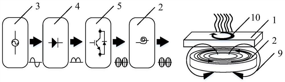
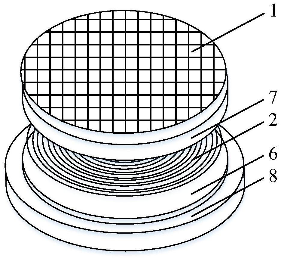
[0053] This embodiment provides a direct induction heating device for a wafer, see Figure 1 to Figure 2 , comprising an alternating magnetic flux generating component, using the alternating current of the alternating magnetic beam generating component to generate an alternating magnetic flux 9, the wafer 1 is placed in the alternating magnetic beam 9 generated by the alternating magnetic beam generating component, and the wafer placed in the alternating magnetic beam 9 1 generates an eddy current 10, and the eddy current 10 passes through the wafer 1 to generate Joule heat to heat the wafer 1.

[0054]Compared with the prior art, the direct induction heating device of the wafer provided in this embodiment adopts the direct induction heating method, and uses the alternating magnetic beam generating component to generate the alternating magnetic beam 9. Due to the existence of the induced current, it is placed in the alternating magnetic beam The wafer 1 in 9 will generate eddy...

Embodiment 2

[0078] This embodiment provides a method for direct induction heating of a wafer, comprising the following steps:

[0079] Using alternating current to generate alternating magnetic beams, placing the wafer in the alternating magnetic beams, eddy currents are generated in the wafers, and the eddy currents pass through the wafers to generate Joule heat to heat the wafers.

[0080] Compared with the prior art, the beneficial effects of the method for direct induction heating of wafers provided in this embodiment are basically the same as those of the device for direct induction heating of wafers provided in Embodiment 1, and will not be repeated here.

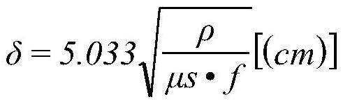
[0081] Specifically, due to the skin effect, the surface of the wafer will be heated intensively. By adjusting the frequency of the alternating magnetic beam 9, the penetration depth can be adjusted. The higher the frequency of the alternating current, the lower the penetration depth. Therefore, the above heating method also inclu...


PUM


Abstract

The invention discloses a direct induction heating device and a heating method of a wafer, belongs to the technical field of semiconductors, and is used for solving the problems of low heating speed and uncontrollable heating depth of an indirect induction heating mode of the wafer in the prior art. The direct induction heating device for the wafer comprises an alternating magnetic bundle generation assembly, alternating current of the alternating magnetic bundle generation assembly is used for generating an alternating magnetic bundle, the wafer is arranged in the alternating magnetic bundle generated by the alternating magnetic bundle generation assembly, eddy current is generated in the wafer arranged in the alternating magnetic bundle, and joule heat is generated by the eddy current through the wafer to heat the wafer. The direct induction heating method of the wafer comprises the following steps: generating an alternating magnetic bundle by using alternating current, placing the wafer in the alternating magnetic bundle, generating eddy current in the wafer, generating joule heat by the eddy current through the wafer, and heating the wafer. The direct induction heating device and the heating method of the wafer can be used for direct induction heating of the wafer.

Description

technical field [0001] The invention belongs to the technical field of semiconductors, and in particular relates to a direct induction heating device and a heating method for wafers. Background technique [0002] In the semiconductor manufacturing process, it is necessary to repeatedly etch to form a narrow and deep hole, and then use a planarization process to fill the hole. In the above process, because the wafer temperature will affect the product yield, it is necessary to maintain an appropriate The wafer temperature is very important. In the etching process, according to the requirement of maintaining the uniform temperature of the whole wafer, it is divided into two or more temperature control areas, requiring the use of fine temperature control technology. With the miniaturization of the semiconductor manufacturing process, the holes that need to be etched are deeper and narrower than before. In order to improve the profile of the holes, various efforts are required....

Claims


Application Information

Patent Timeline
Patent Type & Authority Applications(China)
IPC IPC(8): H05B6/10H05B6/36H05B1/02H05B3/00G03F7/20
CPCH05B6/10H05B6/36H05B1/0233H05B3/0047G03F7/70875Y02P10/25
Inventor 郑宇现周娜李琳王佳李俊杰
Owner INST OF MICROELECTRONICS CHINESE ACAD OF SCI
Why Eureka
Try Eureka