Double-gate ferroelectric transistor, preparation method and data erasing and reading method

A technology of ferroelectric transistors and gate electrodes, which is applied in semiconductor/solid-state device manufacturing, circuits, electrical components, etc., can solve the problems of not meeting the application requirements of high-performance devices, limited fatigue times of transistors, and poor anti-fatigue characteristics. Small programming and erasing voltages and operating voltages, avoiding voltage division, and improving the effect of anti-fatigue characteristics

Pending Publication Date: 2022-05-24
XIDIAN UNIV
View PDF0 Cites 1 Cited by
  • Summary
  • Abstract
  • Description
  • Claims
  • Application Information

AI Technical Summary

Problems solved by technology

[0003] However, there is a big gap in the anti-fatigue characteristics of ferroelectric field effect transistors based on HfO2 thin films compared with traditional perovskite ferroelectric materials, which cannot meet the application requirements of high-performance devices.
[0004] The traditional data erasing / reading method is to apply erasing / reading pulses on the source, drain and gate, so the insulating layer will withstand a higher electric field due to the small dielectric constant during pulse erasing, resulting in breakdown , so that the ferroelectric field effect transistor based on HfO2 thin film has limited fatigue times and poor fatigue resistance

Method used


Image

  • Double-gate ferroelectric transistor, preparation method and data erasing and reading method
  • Double-gate ferroelectric transistor, preparation method and data erasing and reading method
  • Double-gate ferroelectric transistor, preparation method and data erasing and reading method

Examples


Embodiment 1

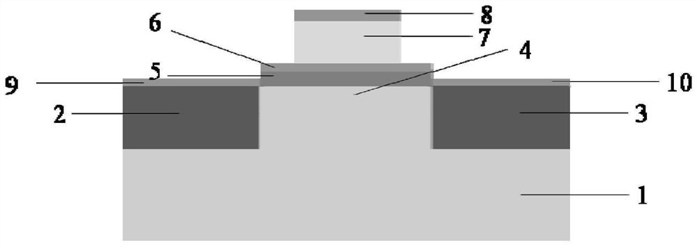
[0038] like figure 1 As shown, the present invention discloses a dual-gate ferroelectric transistor, comprising a substrate 1 and a channel 4, the channel 4 is arranged above the substrate and in the middle of the substrate, and the channels 4 are respectively arranged on both sides There are a source region 2 and a drain region 3; the source region 2 is provided with a source electrode 10, the drain region 3 is provided with a drain electrode 9, and the channel 4 is sequentially provided with Insulation layer 5 , lower gate electrode 6 , ferroelectric gate dielectric layer 7 and upper gate electrode 8 .

[0039] figure 1 The double-gate ferroelectric transistor can be obtained according to the preparation method of implementation 2. Those skilled in the art can also use other methods to obtain figure 1 Structure of a double-gate ferroelectric transistor. The insulating layer 5 will carry a relatively high voltage in conventional technical means and is easily broken down. ...

Embodiment 2

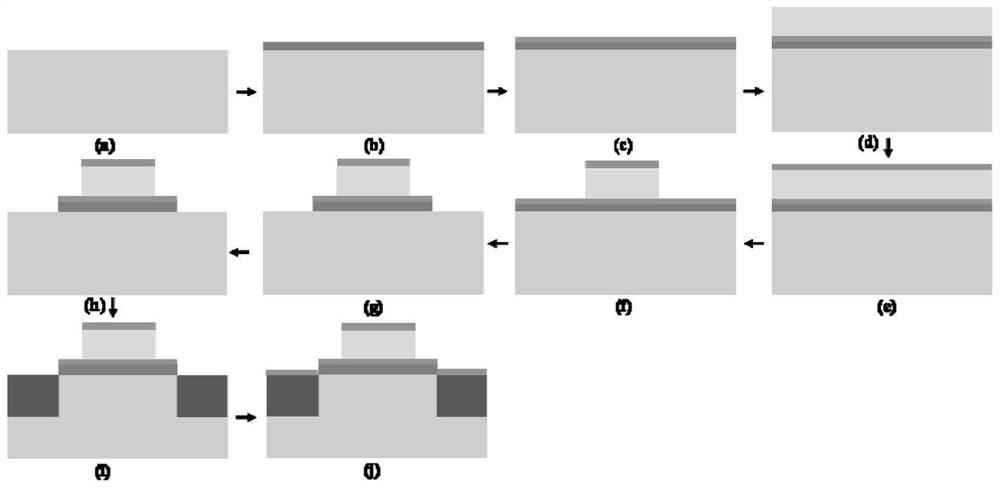
[0052] see image 3 , the invention discloses a preparation method of a double-gate ferroelectric transistor, comprising:

[0053] The substrate 1 is cleaned, and a SiO2 insulating layer 5 is grown on the substrate 1 through a dry oxygen process, see image 3 (a)(b);

[0054] A magnetron sputtering process is used to deposit TaN on the SiO2 insulating layer 5 to form a lower gate electrode 6, see image 3 (c);

[0055] A HfZrOx film is deposited on the lower gate electrode 6 to form a ferroelectric gate dielectric layer 7, see image 3 (d);

[0056] The magnetron sputtering process is used to deposit TaN on the ferroelectric gate dielectric layer 7 to form the upper gate electrode 8, see image 3 (e);

[0057] Using a photolithography process, the region of the upper gate electrode 8 is marked on the upper gate electrode 8;

[0058] Using an etching process, the excess parts around the area of ​​the upper gate electrode 8 are etched to the surface of the lower gate elec...

Embodiment 3

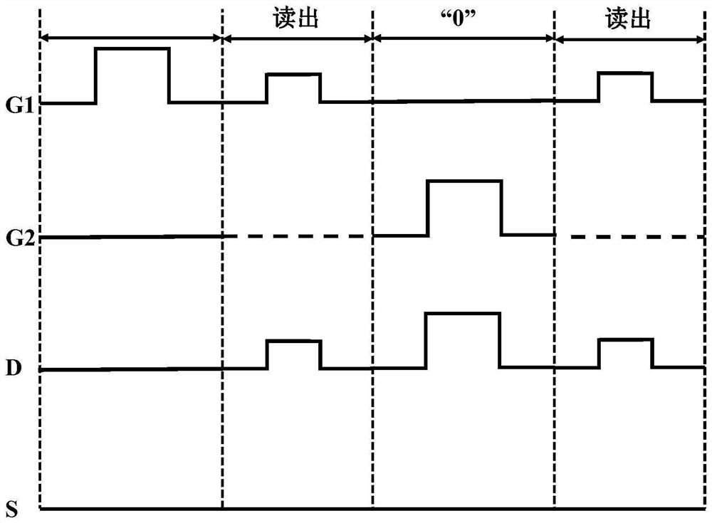
[0079] The switching electrode type data erasing / reading method of the present invention is realized based on the double-gate ferroelectric field effect transistor of the structure of the first embodiment. The timing diagram of the voltage changing with time for erasing and reading is as follows figure 2 As shown, the voltage waveform of the upper gate electrode 8 corresponds to G1, the voltage waveform of the lower gate electrode 6 corresponds to G2, the voltage waveform of the source electrode 10 corresponds to S, and the voltage waveform of the drain electrode 9 corresponds to D.

[0080] The invention discloses a data erasing, writing and reading method, applying the double-gate ferroelectric transistor described in Embodiment 1,

[0081] When writing data: a positive pulse voltage is applied between the upper gate electrode 8 and the lower gate electrode 6, the source electrode 10 is grounded, the potential of the drain electrode 9 and the lower gate electrode 6 are kept...


PUM

PropertyMeasurementUnit
thicknessaaaaaaaaaa
thicknessaaaaaaaaaa

Abstract

The invention belongs to the technical field of transistors, and discloses a double-gate ferroelectric transistor, a preparation method and a data erasing and reading method.The double-gate ferroelectric transistor comprises a substrate and a channel, the channel is arranged above a lining body and located in the middle of the lining body, and a source electrode region and a drain electrode region are arranged on the two sides of the channel respectively; a source electrode is arranged on the source electrode region, a drain electrode is arranged on the drain electrode region, and an insulating layer, a lower gate electrode, a ferroelectric gate dielectric layer and an upper gate electrode are sequentially arranged above the channel from bottom to top. The dual-gate ferroelectric field transistor has the beneficial effects that the erasing process is realized by adding pulses between the upper gate electrode and the lower gate electrode, so that voltage is prevented from falling on the insulating layer; the breakdown of the insulating layer caused by an overlarge electric field on the insulating layer is avoided, and the anti-fatigue property of the transistor is improved; and voltage division of the insulating layer can be avoided, so that the programming and erasing voltage and the working voltage of the ferroelectric field effect transistor are reduced.

Description

technical field [0001] The invention relates to the technical field of transistors, in particular to a double-gate ferroelectric transistor, a preparation method and a data erasing and reading method. Background technique [0002] As a device for storing electronic system information, semiconductor memory is the core component to ensure the normal operation of the system, and its requirements are high storage density, fast writing speed, low power consumption, many rewritable times, and stable storage state. Among ferroelectric memories, ferroelectric field effect transistors (FeFETs) offer many distinct advantages, including non-volatile data storage, program / erase times in the nanosecond range, low operating voltages, virtually unlimited endurance, and lossless readout out. [0003] However, the anti-fatigue properties of ferroelectric field effect transistors based on HfO2 films are far behind traditional perovskite ferroelectric materials, which cannot meet the applicat...

Claims


Application Information

Patent Timeline
Patent Type & Authority Applications(China)
IPC IPC(8): H01L29/78H01L21/336G11C11/22
CPCH01L29/78391H01L29/6684G11C11/223G11C11/2273G11C11/2275
Inventor 彭悦肖文武张悦媛韩根全
Owner XIDIAN UNIV
Why Eureka
Try Eureka