Solar silicon wafer reworking and inserting machine and implementation method thereof
A technology of solar silicon wafers and inserting machines, which is applied in the direction of conveyor objects, sustainable manufacturing/processing, climate sustainability, etc., and can solve problems such as manual operations that cannot meet the needs of production, silicon wafer pollution, and prone to fragmentation , to achieve the effect of low labor intensity, high degree of automation, and improved feeding efficiency
- Summary
- Abstract
- Description
- Claims
- Application Information
AI Technical Summary
Problems solved by technology
Method used
Image
Examples
Embodiment 1
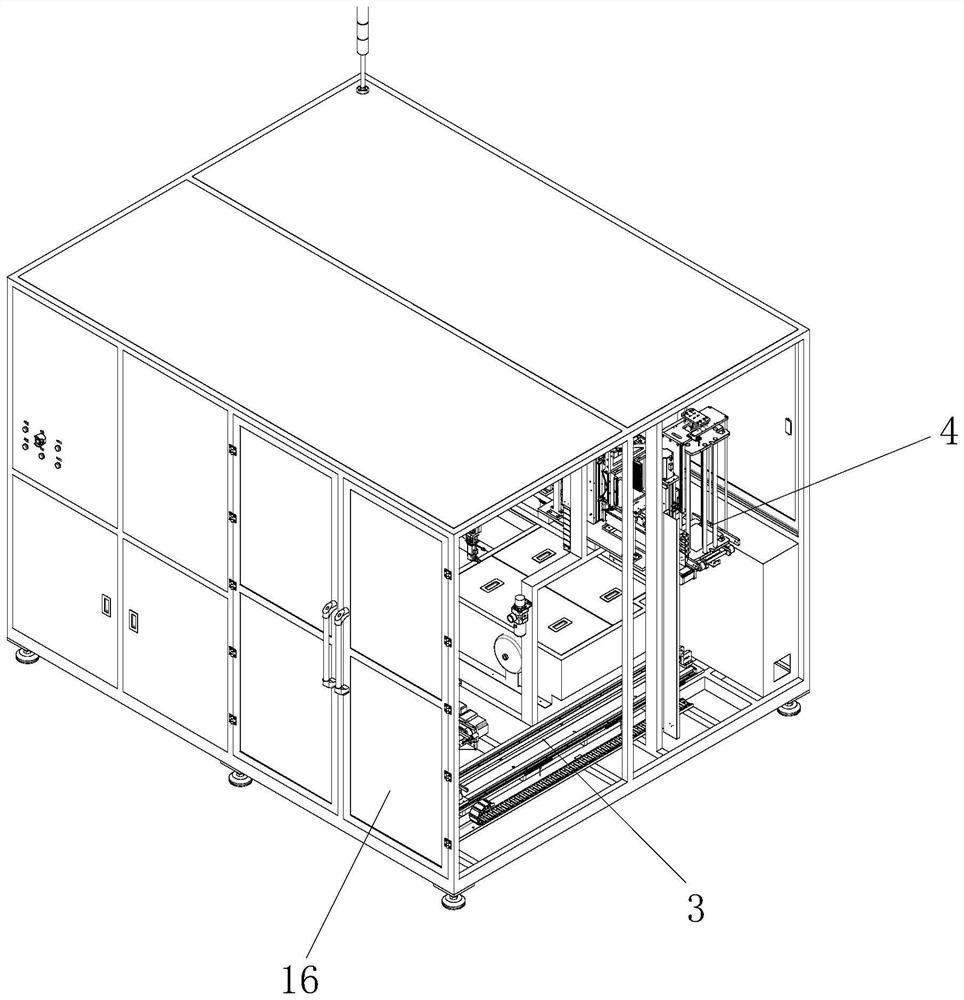
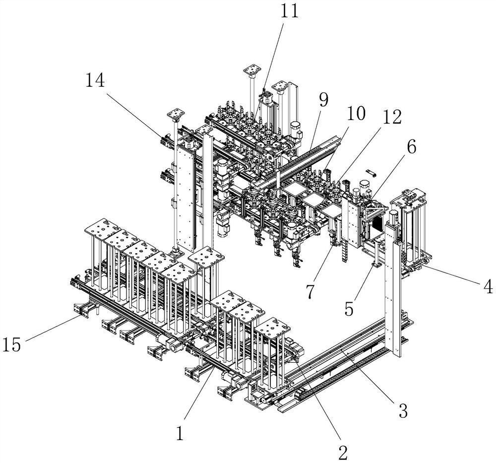
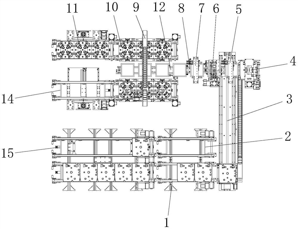
[0053] see Figure 1-18 , the present invention provides the following technical solutions: a solar silicon wafer rework inserting machine, comprising a bin belt lifting switching mechanism 11, the end of the bin belt lifting switching mechanism 11 is provided with a first silicon wafer feeding belt 10, the first One side of the silicon wafer feeding belt 10 is provided with a stepping belt 12, and the top of the stepping belt 12 and the first silicon wafer feeding belt 10 is provided with a silicon wafer feeding mechanism 9, and one side of the stepping belt 12 discharge end is provided with Silicon chip feeding belt 8 is arranged, and the top of silicon chip feeding belt 8 feeding end is provided with second positioning mechanism 7, and one side of silicon chip feeding belt 8 discharging end is provided with flower basket lifting mechanism 4, and the side of flower basket lifting mechanism 4 is provided with There is a flower basket horizontal moving mechanism 3, the side of...
Embodiment 2
[0072] The difference between this embodiment and Embodiment 1 is that specifically, the silicon wafer feed belt 8 also includes a top material belt 83, a first positioning mechanism 5 is arranged above the top material belt 83, and the top material belt 83 is arranged on the feed belt 82 Below the output end, the bottom of the top material belt 83 is provided with a top material belt installation plate 89, the bottom of the top material belt installation plate 89 is provided with a top material belt installation bottom plate 87, the top material belt installation plate 89 and the top material belt installation bottom plate 87 Through the sliding connection of the jacking belt guide rod 88, the top of the jacking belt installation base plate 87 is provided with a jacking belt cylinder 86, and the output end of the jacking belt cylinder 86 is connected with the jacking belt mounting plate 89.
[0073] By adopting the above-mentioned technical solution, the silicon wafer is repos...
Embodiment 3
[0075] The difference between this embodiment and Embodiment 1 is that: specifically, the side of the stepping belt 12 away from the first silicon wafer feeding belt 10 is provided with a second silicon wafer feeding belt, and the second silicon wafer feeding belt feeds One side of the end is provided with a bin belt lift and traverse switching mechanism 14.
[0076] By adopting the above technical scheme, after the silicon wafers on the first silicon wafer feeding belt 10 are taken out, the second silicon wafer feeding belt is used for feeding, so as to realize non-stop feeding and improve the feeding efficiency of silicon wafers.
[0077] Specifically, the bin belt lift and traverse switching mechanism 14 includes two second bin belt support guide rods 141, wherein a second lift switching module 142 is provided at the middle position of the two second bin belt support guide rods 141 , the output end of the second lifting switching module 142 is provided with two lifting plat...
PUM
 Abstract
Description
Claims
Application Information


