
IGBT device structure

A device structure, a pair of technologies, applied in the direction of semiconductor devices, electrical components, circuits, etc., can solve the problems of process difficulty and stress increase, and achieve the effect of increasing doping concentration and simple structure

Active Publication Date: 2022-06-21
NANTONG SANRISE INTEGRATED CIRCUIT CO LTD
View PDF3 Cites 0 Cited by
  • Summary
  • Abstract
  • Description
  • Claims
  • Application Information

AI Technical Summary

Problems solved by technology

However, reducing the distance Pitch between adjacent cells of the IGBT will bring great difficulty to the process, and the stress will also increase

Method used


Image

  • IGBT device structure
  • IGBT device structure
  • IGBT device structure

Examples


Embodiment Construction

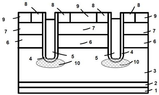
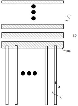
[0032] As a further improvement, the terminal also has a horizontal connection portion 20b vertically connected to both ends of the bottom ring 20a, and the top second conductivity type ion implantation region is also connected to the bottom ring 20a via the horizontal connection portion 20b. connect.

[0033] As a further improvement, the terminal has: the groove has a widened area 32, the widened area 32 overlaps with the connecting area of ​​the horizontal connecting portion 20b, and a through hole 33 is arranged in the widened area 32 , the through hole 33 is connected to the ion implantation region 10 of the second conductivity type located at the bottom of the trench.

[0034] As a further improvement, in an adjacent pair of the grooves, the adjacent pair of the widened regions 32 are arranged in a staggered manner, so as to reduce the overall width of the adjacent pair of the grooves.

[0035] As a further improvement, the widened regions 32 of all the grooves are merg...


PUM


Abstract

The invention discloses an IGBT (Insulated Gate Bipolar Translator) device structure, the distance between adjacent cells of adjacent grooves is a standard fixed value, a second conduction type ion implantation region arranged around the bottoms of the grooves is also arranged in a first conduction type drift region, and the depletion of a carrier storage layer CS comprises: transverse depletion of the grooves, transverse depletion of the first conduction type drift region, transverse depletion of the second conduction type drift region, transverse depletion of the second conduction type drift region, transverse depletion of the second conduction type drift region and transverse depletion of the third conduction type drift region. The longitudinal depletion of the second conductive type channel and the depletion of the second conductive type ion implantation region enable the carrier storage layer CS to be completely depleted when the concentration of the carrier storage layer CS is increased. According to the invention, the ion implantation at the bottom can also be depleted, even if the concentration of CS is increased, the CS can be completely depleted, and the performance and application environment of the semiconductor device can be improved with low cost.

Description

technical field [0001] The invention relates to semiconductor devices, in particular to an IGBT device structure. Background technique [0002] In the field of semiconductor devices, IGBTs are common and important devices. IGBT (Insulated Gate Bipolar Transistor), that is, insulated gate bipolar transistor, is a composite fully-controlled voltage-driven power semiconductor device composed of BJT (bipolar transistor) and MOS (insulated gate field effect transistor), with MOSFET The advantages of high input impedance and low conduction voltage drop of GTR. The saturation voltage of GTR is low, the carrying current density is large, but the driving current is large; the driving power of MOSFET is small, the switching speed is fast, but the conduction voltage drop is large, and the current carrying density is small. The IGBT combines the advantages of the above two devices, with low driving power and low saturation voltage. It is very suitable for the conversion system with a...

Claims


Application Information

Patent Timeline
IPC IPC(8): H01L29/06H01L29/739
CPCH01L29/0684H01L29/7393
Inventor 曾大杰
Owner NANTONG SANRISE INTEGRATED CIRCUIT CO LTD
Features
  • Generate Ideas
  • Intellectual Property
  • Life Sciences
  • Materials
  • Tech Scout
  • Unparalleled Data Quality
  • Higher Quality Content
  • 60% Fewer Hallucinations
Learn More