Preparation method of strippable ultrathin carrier copper foil

A technology of carrier copper foil and ultra-thin copper foil, which is used in the manufacture of printed circuits, the manufacture of printed circuit precursors, printed circuits, etc. Complete and other problems, to achieve the effect of low cost of technical transformation, enhanced bonding force, and satisfactory peel strength

Pending Publication Date: 2022-06-24
UNIV OF ELECTRONICS SCI & TECH OF CHINA
View PDF7 Cites 1 Cited by
  • Summary
  • Abstract
  • Description
  • Claims
  • Application Information

AI Technical Summary

Problems solved by technology

[0005] The technical problem to be solved by the present invention is to provide a preparation method of ultra-thin carrier copper foil for the problems of unstable peel strength, incomplete peeling of copper foil, wrinkles and curls in the existing ultra-thin copper foil,
The surface of each layer of the ultra-thin carrier copper foil is uniform and flat, the performance is stable, and the peeling layer has good conductivity. It is difficult to form a uniform thickness when laminating at high temperature, and it is difficult to peel off after the ultra-thin copper foil diffuses into the peeling layer

Method used


Image

  • Preparation method of strippable ultrathin carrier copper foil
  • Preparation method of strippable ultrathin carrier copper foil
  • Preparation method of strippable ultrathin carrier copper foil

Examples


preparation example Construction

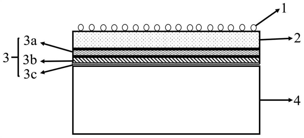
[0042] A preparation method of a peelable ultra-thin carrier copper foil, the copper foil sequentially comprises a carrier copper foil 4 with a thickness of 12-35 μm, a peeling layer 3, an ultra-thin copper foil layer 2 and a roughening layer 1 from bottom to top, and the composite peeling Layer 3 includes, from bottom to top, an immersion metal layer 3c, an organic barrier layer 3b, and a peeling layer 3a, and the preferred thickness of the ultra-thin copper foil is 4-6 μm.

[0043] Preparation includes the following steps:

[0044] (1) Preparation of cathode: Select double-sided copper foil for printed circuit board manufacturing as carrier copper foil, and perform micro-etching and pickling treatment on the smooth surface of carrier copper foil to obtain oxide-free and clean copper foil surface, All surface treatments are done on the smooth surface of the carrier copper foil;

[0045] (2) Preparation of immersion metal layer

[0046] The surface-treated carrier copper foi...

Embodiment 1

[0066] A preparation method of peelable ultra-thin carrier copper foil, comprising the following steps:

[0067] (1) Preparation of cathode: Cut a piece of 100mm×50mm wide 18μm double-sided copper foil for printed circuit board manufacturing with scissors, one of which is matte and the other is smooth. The surface treatments of all the following examples are on the smooth surface. The above-mentioned copper foil is subjected to micro-etching treatment and pickling treatment in turn to achieve the purpose of removing surface oxides and impurities, and then washed with deionized water to prepare for use.

[0068] (2) Preparation of immersion metal layer

[0069] Immersion metal layer on the surface of the carrier copper foil: Immerse the cleaned carrier copper foil in a mixed solution of 20g / L stannous chloride, 80g / L hydrochloric acid, and 50g / L sodium hypophosphite in sequence, and soak for 1min at 60°C After washing with deionized water, it was immersed in a hydrogen peroxid...

Embodiment 2

[0085] A preparation method of peelable ultra-thin carrier copper foil, comprising the following steps:

[0086] (1) Preparation of cathode: Cut a piece of 100mm×50mm wide 18μm double-sided copper foil for printed circuit board manufacturing with scissors, one of which is matte and the other is smooth. The surface treatments of all the following examples are on the smooth surface. The above-mentioned copper foil is subjected to micro-etching treatment and pickling treatment in turn to achieve the purpose of removing surface oxides and impurities, and then washed with deionized water to prepare for use.

[0087] (2) Preparation of immersion metal layer

[0088] Immersion metal layer on the surface of the carrier copper foil: Immerse the cleaned carrier copper foil in a mixed solution of 20g / L stannous chloride, 80g / L hydrochloric acid, and 50g / L sodium hypophosphite in sequence, and soak for 1min at 60°C After washing with deionized water, it was immersed in a hydrogen peroxid...


PUM

PropertyMeasurementUnit
thicknessaaaaaaaaaa
thicknessaaaaaaaaaa
concentrationaaaaaaaaaa

Abstract

The invention relates to a preparation method of a strippable ultrathin carrier copper foil, and provides a key material for a 5G communication high-frequency and high-speed printed circuit board. According to the strippable ultrathin carrier copper foil, the 18-micron carrier copper foil, the dip-plated metal layer, the organic barrier layer, the stripping layer, the ultrathin copper foil layer and the coarsening layer are sequentially arranged, the dip-plated metal layer can reduce equipotential points of a copper surface, the binding force of the carrier copper foil and the organic layer is enhanced, and the requirement for anti-stripping strength is met; the organic layer and the metal layer are jointly used as a stripping layer, so that the problems that a single organic layer easily causes poor conductivity and non-uniform thickness during electro-deposition of an ultrathin copper foil layer and is easily separated from a carrier before use can be solved. The thickness of the ultrathin carrier copper foil prepared by the method is about 5 microns, the ultrathin carrier copper foil can be successfully stripped, and no copper powder or stripping layer is left on the surface of the ultrathin carrier copper foil.

Description

technical field [0001] The invention belongs to the field of electronic information materials, in particular to a peelable ultra-thin carrier copper foil and a preparation method thereof. Background technique [0002] In the current environment of rapid development of the 5G industry, the PCB industry is booming due to its influence. From the perspective of the downstream application industry of PCB, communications, mobile phones, servers, data storage and automobiles will become the best segments of PCB in the future in the next five years. On the track, the demand for high-end PCB products such as corresponding multi-layer boards, HDI, flexible boards and IC packaging substrates will be very obvious; at the same time, from the upstream of the industry chain, as an indispensable electrolytic copper foil in the industry chain, it is 5G communication. The key material of high-frequency and high-speed printed circuit boards, whether in raw material copper clad laminates or in ...

Claims


Application Information

Patent Timeline
Patent Type & Authority Applications(China)
IPC IPC(8): C25D3/38C25D5/34C25D7/00H05K3/02
CPCC25D3/38C25D7/00C25D5/34H05K3/022
Inventor 周国云文雯罗宇兴于鹏鹏何为王守绪王翀杨文君
Owner UNIV OF ELECTRONICS SCI & TECH OF CHINA
Why Eureka
Try Eureka