Semiconductor light-emitting element

A light-emitting element and semiconductor technology, applied in semiconductor devices, electrical components, circuits, etc., can solve problems such as chip burn and aggravate current congestion, achieve the effects of reducing the impact of brightness, improving performance, and avoiding overall widening design

Pending Publication Date: 2022-06-28
XIAMEN SANAN OPTOELECTRONICS CO LTD
View PDF0 Cites 0 Cited by
  • Summary
  • Abstract
  • Description
  • Claims
  • Application Information

AI Technical Summary

Problems solved by technology

When the light-emitting diode is just powered on, it will generate a transient high load current, which is more likely to aggravate the current crowding, and the chip burn is more likely to occur at the connection between the electrode lead connection section and the extension section

Method used


Image

  • Semiconductor light-emitting element
  • Semiconductor light-emitting element
  • Semiconductor light-emitting element

Examples


Embodiment 1

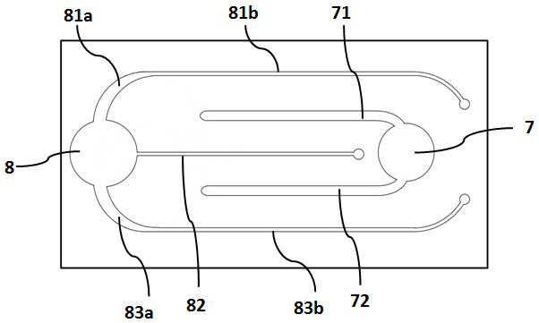
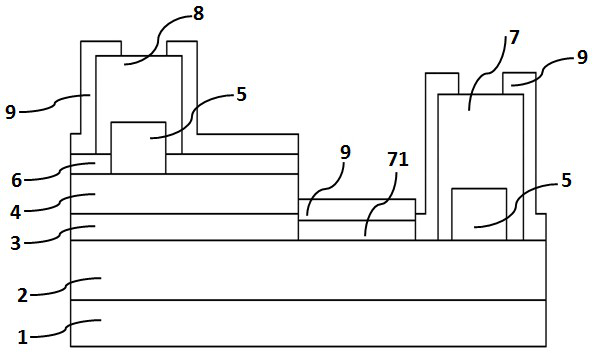
[0050] This embodiment provides the following semiconductor light-emitting element, figure 2 It is a schematic cross-sectional view of a semiconductor light-emitting element, which includes: 1: substrate; 2: first conductive type semiconductor layer; 3: active layer; 4: second conductive type semiconductor layer; 5: current blocking layer; 6: transparent conductive layer 7: first electrode; 71, 72: first electrode lead; 8: second electrode; 81, 82, 83: second electrode lead; 9: insulating protective layer.

[0051] The substrate 1 may be an insulating substrate or a conductive substrate. Substrate 1 is a growth substrate for epitaxial growth of semiconductor barrier crystal stacks, including sapphire (Al 2 O 3 ) or spinel (MgA1 2 O 4 ) insulating substrates; silicon carbide (SiC), ZnS, ZnO, Si, GaAs, diamond; and oxide substrates such as lithium niobate and niobium gallate that are lattice-matched with nitride semiconductors. The substrate 1 includes a first surface, a s...

Embodiment approach

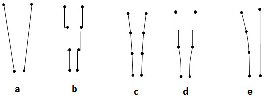
[0065] The second electrode 8 has a plurality of electrode leads, and at least one second electrode lead includes a connecting section connected to the second electrode, and an extension section extending from the connecting section to the first electrode; the second electrode lead extends The segment has a first portion extending from the second electrode lead connection segment to gradually approaching the first electrode and a second portion extending from the first portion and gradually approaching the first electrode, and the width of the first portion is gradually changed in the extending direction, so The width of the second part is fixed. As an embodiment of the present invention, the width of the first portion of the second electrode extension segment can be linearly narrowed at a fixed rate of change from the extension direction, such as image 3 As shown in a; as another embodiment of the present invention, the width of the first part of the second electrode extensi...

Embodiment 2

[0084] In this example, as Figure 9 As shown, the difference from Embodiment 1 is that the two lead wires 81 and 83 of the p-electrode of this embodiment do not have the ends as in Embodiment 1, and other parts are the same.


PUM


Abstract

A semiconductor light emitting element includes: a first conductive type semiconductor layer and a second conductive type semiconductor layer; a first electrode and a second electrode disposed on the first conductive type semiconductor layer and the second conductive type semiconductor layer, respectively, and located on the same surface side of the semiconductor light emitting element; the at least one second electrode lead comprises a connecting section connected with the second electrode and an extending section extending from the connecting section to the first electrode; the first part extends from the second electrode lead connecting section to be gradually close to the first electrode, the second part extends from the first part to be gradually close to the first electrode, and the width of the first part is gradually reduced from the extending direction. And the width of the second part is fixed. The width of the first part of the extending section of the second electrode lead is gradually reduced from the extending direction, so that the overvoltage impact performance (EOS performance) of the semiconductor light-emitting element can be improved.

Description

technical field [0001] The invention relates to a semiconductor light-emitting element, which belongs to the technical field of semiconductor optoelectronics. Background technique [0002] Light Emitting Diode (LED for short) has the advantages of high luminous intensity, high efficiency, small size and long service life, and is considered to be one of the most potential light sources at present. In recent years, LEDs have been widely used in daily life, such as lighting, signal display, backlight, car lights and large-screen displays, etc. At the same time, these applications also put forward higher requirements for the brightness and luminous efficiency of LEDs. [0003] In order to improve the luminous efficiency of LEDs, the design of LED chips is not only optimized for small electrodes, but also for thin electrode leads, so as to reduce the light-blocking area and improve the luminous brightness. However, at a large current density, the thin electrode lead is easy to c...

Claims


Application Information

Patent Timeline
Patent Type & Authority Applications(China)
IPC IPC(8): H01L33/62H01L33/64
CPCH01L33/62H01L33/647
Inventor 陈思河王锋王绘凝贺春兰洪灵愿彭康伟
Owner XIAMEN SANAN OPTOELECTRONICS CO LTD
Why Eureka
Try Eureka