Curved-surface battery and packaging method thereof
A packaging method and curved surface technology, applied in the direction of circuits, electrical components, electric solid devices, etc., can solve problems such as damage and affecting the practical application of perovskite solar cell packaging technology, and achieve the effect of meeting technical requirements and good water vapor
- Summary
- Abstract
- Description
- Claims
- Application Information
AI Technical Summary
Problems solved by technology
Method used
Image
Examples
Embodiment 1
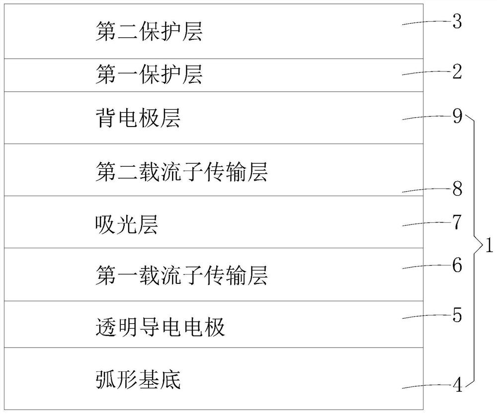
[0039] The first embodiment of the packaging method for a curved battery of the present invention includes the following steps:
[0040] Step 11. Printing of the substrate: the material of the substrate is an aluminum plate. The heated aluminum wire is punched out through a nozzle with a diameter of 0.5mm, and the printing parameters are set to 100% filling to form the target structure model. The printing parameters can be adjusted with different structure models.
[0041] Step 12. Printing of the back electrode layer: the material of the back electrode layer is metallic silver. The silver nanoparticle ink is printed by aerosol (ultrasonic atomization spraying). The ultrasonic atomization device atomizes the ink and sprays it with nitrogen flow. The flow rate is set to 20sccm. After printing, it is dried in an atmosphere of 80 ℃ for 30min to form a silver back electrode. Floor.
[0042] Step 13, printing of the first carrier transport layer: the material of the first carrier...
Embodiment 2
[0049] The second embodiment of the packaging method for a curved battery of the present invention includes the following steps:
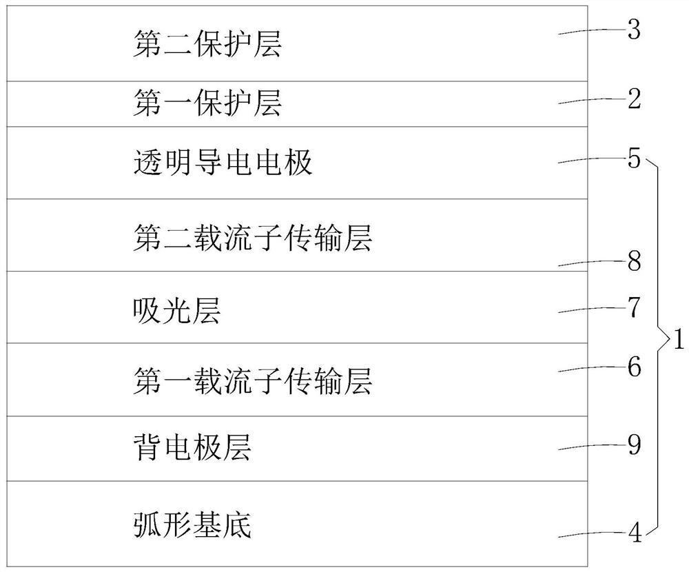
[0050] Step 21. Printing of the base: the base material is ABS. The heated ABSplus-P430 thermoplastic filament is punched out through a 0.5mm nozzle, and the printing parameters are set to 100% filling to form the target structure model. The printing parameters can be adjusted with different structure models.
[0051] Step 22. Printing of the back electrode layer: the same as step 12.
[0052] Step 23, printing of the first carrier transport layer: the same as step 13.
[0053] Step 24: Printing of the light absorbing layer: the same as step 14.
[0054] Step 25, printing of the second carrier transport layer: the same as step 15.
[0055] Step 26, printing of transparent conductive electrodes: the same as step 16.
[0056] Step 27, printing of the first protective layer: the same as step 17.
[0057] Step 28. Printing of the second protective l...
PUM
| Property | Measurement | Unit |
|---|---|---|
| wavelength | aaaaa | aaaaa |
Abstract
Description
Claims
Application Information


