Packaging structure, photoelectric device and preparation method thereof

A packaging structure, photoelectric device technology, applied in the direction of circuits, electrical components, electrical solid devices, etc., can solve the problems of poor water and oxygen isolation effect, achieve the effects of less surface defect states, reduce production costs, and increase effective diffusion paths

Pending Publication Date: 2022-07-01
TCL CORPORATION
View PDF0 Cites 0 Cited by
  • Summary
  • Abstract
  • Description
  • Claims
  • Application Information

AI Technical Summary

Problems solved by technology

[0006] In view of the above deficiencies in the prior art, the purpose of the present invention is to provide a packaging structure, a photoelectr

Method used


Image

  • Packaging structure, photoelectric device and preparation method thereof
  • Packaging structure, photoelectric device and preparation method thereof
  • Packaging structure, photoelectric device and preparation method thereof

Examples


Embodiment Construction

[0043] The present invention provides an encapsulation structure, an optoelectronic device and a preparation method thereof. In order to make the purpose, technical solution and effect of the present invention clearer and clearer, the present invention is further described in detail below. It should be understood that the specific embodiments described herein are only used to explain the present invention, but not to limit the present invention.

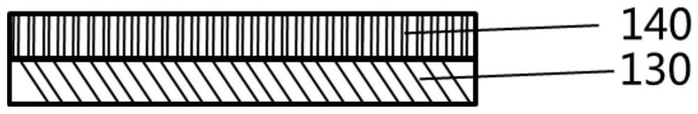
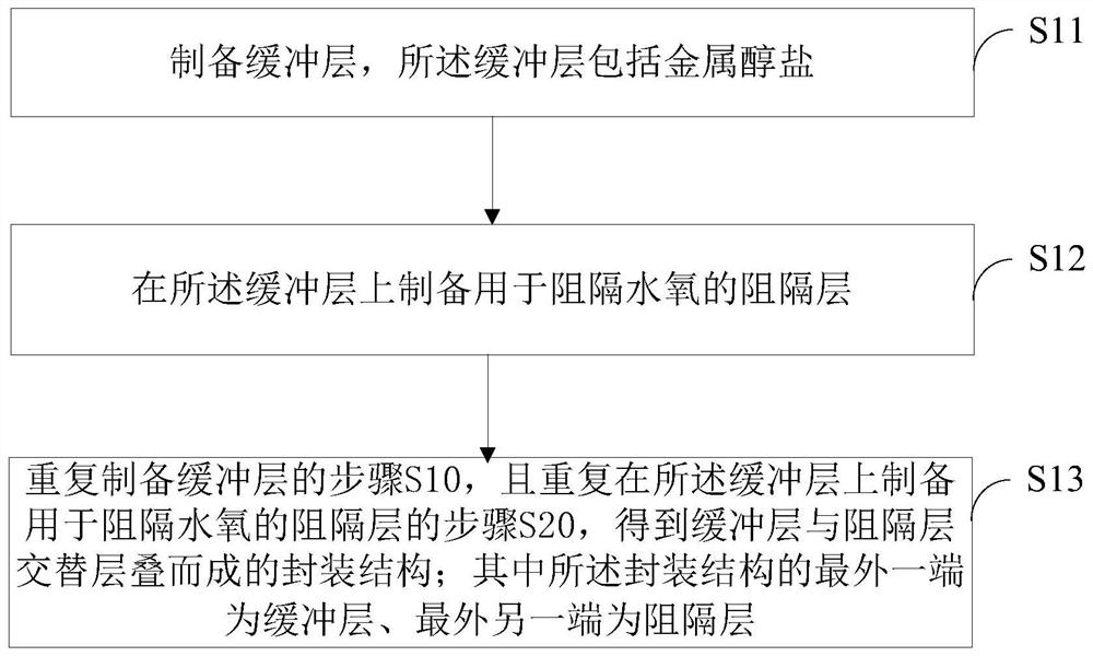
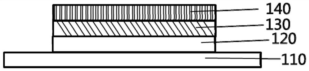
[0044] Embodiments of the present invention provide a packaging structure, such as figure 1 As shown (only one buffer layer and one barrier layer are shown in the package structure in the figure), it includes at least one buffer layer 130 and at least one barrier layer 140, the buffer layers 130 and the barrier layers 140 are alternately stacked and arranged , the buffer layer includes a metal alkoxide, and the barrier layer is used to block water and oxygen.

[0045]It should be noted that the encapsulation structure may be formed ...


PUM


Abstract

The invention discloses a packaging structure, a photoelectric device and a preparation method thereof. The packaging structure comprises at least one buffer layer and at least one blocking layer, the buffer layer and the blocking layer are alternately stacked, the buffer layer comprises metal alkoxide, and the blocking layer is used for blocking water and oxygen. The buffer layer can provide a flat surface for the deposition barrier layer, increase an effective diffusion path and delay water and oxygen permeation, and the unreacted active alkyl and the ultraviolet absorbent left in the buffer layer in the low-temperature process can avoid damage of thermal radiation, oxygen and ultraviolet light in the subsequent process to a photoelectric device. SiOx or SiONx or a composite film layer of the SiOx or the SiONx has fewer film surface defects and lower surface stress, and also has excellent water and oxygen barrier capability. The packaging structure can be prepared through a solution method, is suitable for preparation of large-size devices, improves the utilization rate of packaging materials, and reduces the production cost.

Description

technical field [0001] The invention relates to the technical field of optoelectronic devices, in particular to a packaging structure, an optoelectronic device and a preparation method thereof. Background technique [0002] Optoelectronic devices are semiconductor optoelectronic devices based on organic or inorganic materials, which have a wide range of applications in new energy, sensing, communication, display, lighting and other fields, such as solar cells, photodetectors, OLED / QLED. [0003] The functional layer materials in the structure of optoelectronic devices are very sensitive to pollutants, water, oxygen, etc. in the atmosphere, and are easily eroded by the external environment without isolation protection, which seriously affects the service life of optoelectronic devices. Therefore, optoelectronic devices have higher packaging requirements in practical applications. For example, OLED devices need to meet water vapor permeability ≦10 -6 g / m 2 / day and oxygen pe...

Claims


Application Information

Patent Timeline
IPC IPC(8): H01L51/50H01L51/52H01L51/56
CPCH10K50/115H10K50/8445H10K50/844H10K2102/00H10K71/00H10K50/00H10K50/80
Inventor 王劲杨一行
Owner TCL CORPORATION
Why Eureka
Try Eureka