Manufacturing equipment and process for surface-mounted packaged laser diode

A technology of laser diode and chip packaging, which is applied in the direction of lasers, laser components, semiconductor lasers, etc., can solve problems such as inability to complete automatic loading and unloading, manufacturing and angle adjustment, equipment failure, and electrical components failure, etc., to achieve Convenient angle adjustment, less manual intervention, and high precision

Active Publication Date: 2022-07-12
吉麦思科技(深せん)有限公司
View PDF7 Cites 0 Cited by
  • Summary
  • Abstract
  • Description
  • Claims
  • Application Information

AI Technical Summary

Problems solved by technology

[0009] The object of the present invention is to provide a kind of laser diode manufacturing equipment and technology of SMD packaging, to solve the prior art proposed in the above-mentioned background technology and the above-mentioned cited documents, all cannot complete automatic loading and unloading, manufacturing and angle adjustment, due to electrical The components themselves are small in size and relatively precise, so they require high precision. Once there are more manual steps, the accuracy of the electrical components will be interfered, reducing their durability and increasing minor problems. Once errors occur, the electrical components will be damaged. It is very likely that it cannot be used, causing problems such as the equipment cannot be used normally

Method used


Image

  • Manufacturing equipment and process for surface-mounted packaged laser diode
  • Manufacturing equipment and process for surface-mounted packaged laser diode
  • Manufacturing equipment and process for surface-mounted packaged laser diode

Examples


Embodiment Construction

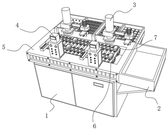
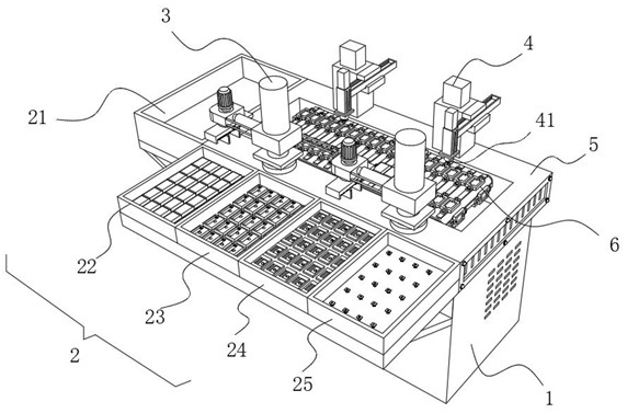
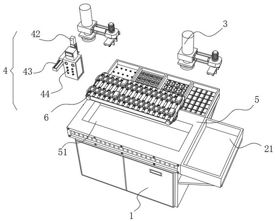
[0050] see Figure 1 to Figure 10 , the present invention provides a kind of technical scheme:

[0051] A chip-packaged laser diode manufacturing equipment, comprising an electrical equipment workbench 5 and an electrical equipment parts main body 7, the top middle of the electrical equipment workbench 5 is provided with an electrical equipment parts conveying assembly 6 for conveying electronic components, and the electrical equipment The top of the worktable 5 is located on one side of the electrical equipment parts conveying assembly 6 and is provided with at least one electrical equipment parts welding machine 4, and the top of the electrical equipment worktable 5 is located on the other side of the electrical equipment parts conveying assembly 6 with at least one electrical equipment parts welding machine 4. An electrical equipment component manufacturing assembly 3 for moving electronic components, the side wall of the electrical equipment workbench 5 close to the electr...


PUM


Abstract

The invention belongs to the technical field of electrical element manufacturing, and discloses surface-mount-packaged laser diode manufacturing equipment which comprises an electrical equipment workbench and an electrical equipment part body. An electrical equipment part conveying assembly used for conveying electronic elements is arranged in the middle of the top end of the electrical equipment workbench; at least one electrical equipment part welding machine is arranged at the top end of the electrical equipment workbench and located on one side of the electrical equipment part conveying assembly. The automation of electronic component manufacturing is greatly improved, the top of the electrical equipment workbench is provided with at least one electrical equipment part manufacturing assembly, the electrical equipment part manufacturing assembly has a double-steering effect, automatic angle alignment can be achieved through an electrical element first-stage motor and an electrical element second-stage motor, and the manufacturing efficiency is improved. After the electrical element clamping structure clamps the electrical equipment part main body, the rotation angle of the electrical element primary motor can be reversely rotated by the electrical element secondary motor.

Description

technical field [0001] The invention belongs to the technical field of electrical component manufacturing, and in particular relates to a laser diode manufacturing equipment and a process for chip packaging. Background technique [0002] In the design of electrical components, diodes are widely used electronic components. In recent years, the design of electronic equipment has become increasingly miniaturized and lightweight, resulting in the volume of electrical components diodes becoming smaller and smaller. [0003] Diode, also known as crystal diode, referred to as diode, is an electronic component with unidirectional conduction current. There is a diode chip inside the SMD diode. One end of this electrical component is connected with a pin, and the other end has an emitting light source. After the pin at one end of the electrical component is in contact with the power supply, the other end of the electrical component can emit a strong light source. [0004] Citation: ...

Claims


Application Information

Patent Timeline
Patent Type & Authority Applications(China)
IPC IPC(8): H01S5/0235H01S5/0236B05D3/02
CPCH01S5/0235H01S5/0236B05D3/0254B05D3/0209
Inventor 王百生魏丽霞
Owner 吉麦思科技(深せん)有限公司
Why Eureka
Try Eureka