Formation method of semiconductor structure

A semiconductor and gate technology, applied in the field of semiconductor structure formation, can solve the problems of difficult channel and poor control ability of the gate structure to the channel, etc.

Pending Publication Date: 2022-07-29
SEMICON MFG INT (SHANGHAI) CORP +1
View PDF0 Cites 0 Cited by
  • Summary
  • Abstract
  • Description
  • Claims
  • Application Information

AI Technical Summary

Problems solved by technology

However, as the channel length of the device is shortened, the distance between the source and the drain of the device is also shortened, so the ability of the gate structure to control the channel becomes worse, and the gate vo...

Method used


Image

  • Formation method of semiconductor structure
  • Formation method of semiconductor structure
  • Formation method of semiconductor structure

Examples


Embodiment Construction

[0029] It can be known from the background art that the devices formed at present still have the problem of poor performance. Now combined with a method of forming a semiconductor structure, the reasons for the poor performance of the device are analyzed.

[0030] refer to Figure 1 to Figure 6 , a schematic diagram of the structure corresponding to each step in a method for forming a semiconductor structure is shown.

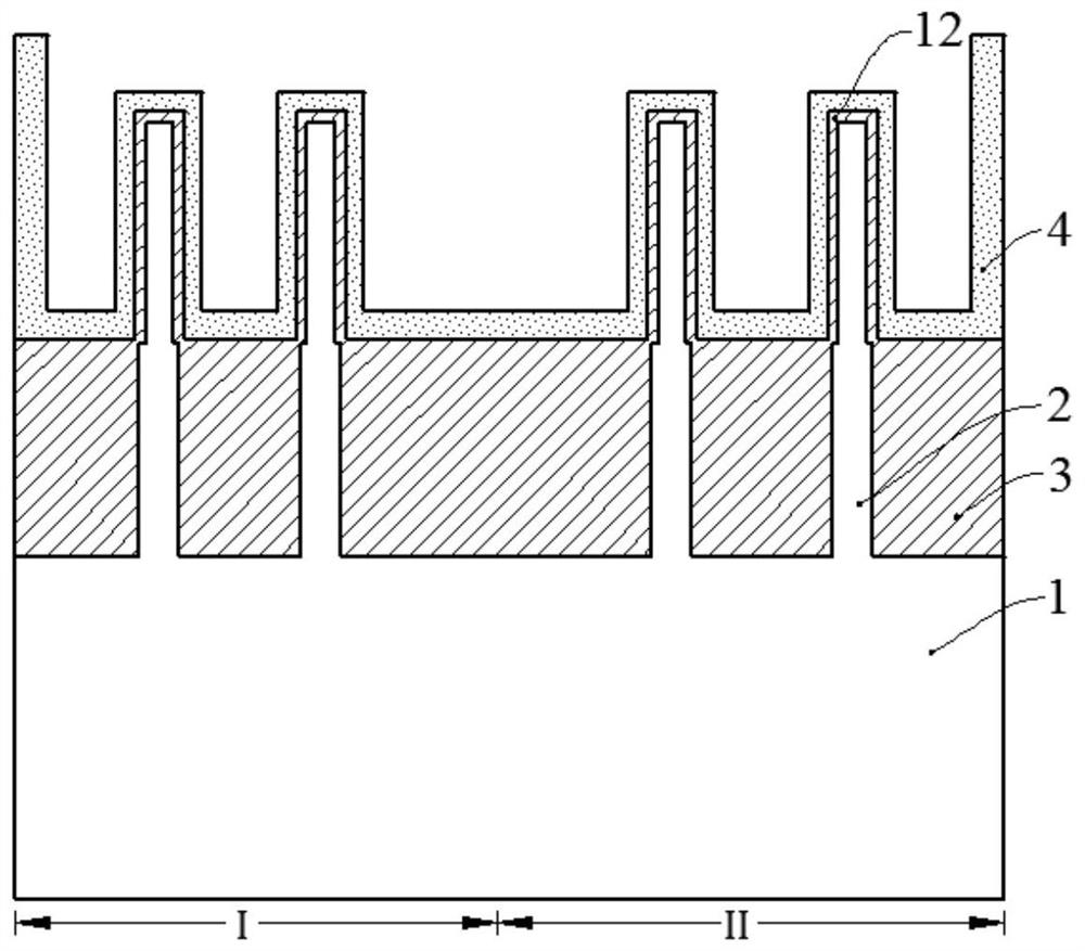
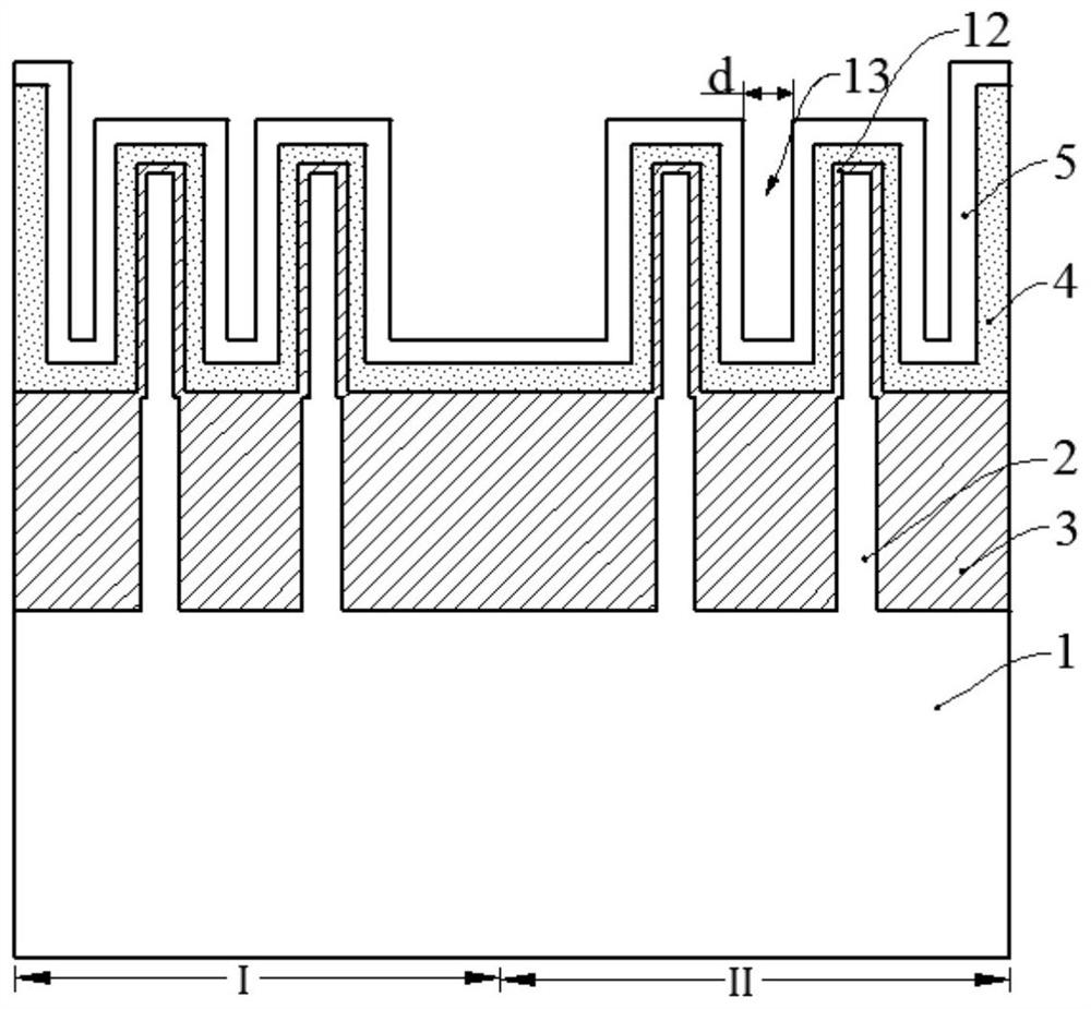
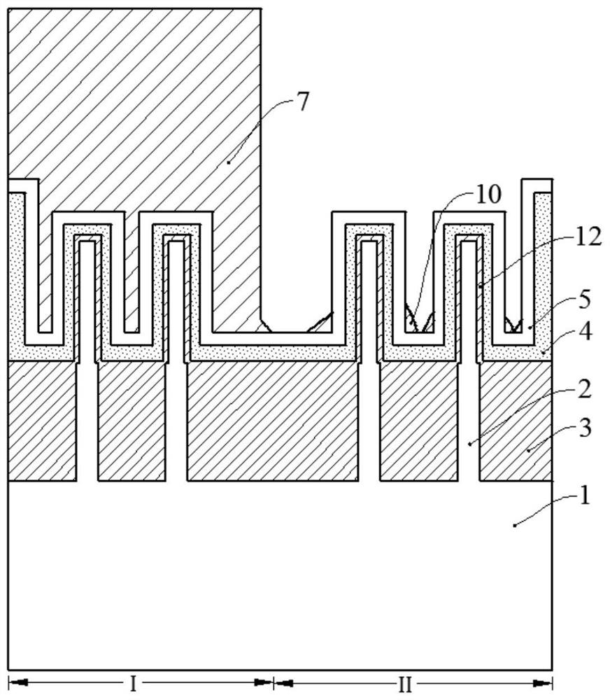
[0031] like figure 1 As shown, a substrate is provided comprising a first region I for forming a PMOS and a second region II for forming an NMOS, the substrate comprising a substrate 1, fins 2 separate from the substrate 1 and an isolation layer 3 covering part of the sidewall of the fin portion 2; an interface layer 12 is formed on the surface of the fin portion 2 exposing the isolation layer 3; after the interface layer 12 is formed, the fin of the isolation layer 3 is exposed The gate dielectric layer 4 is conformally covered on the portion 2 .

[0032] ...


PUM


Abstract

A method for forming a semiconductor structure comprises the following steps: providing a substrate which comprises a first region and a second region, and forming an interlayer dielectric layer with a gate opening on the substrate; a shielding layer covering the gate opening of the second region and exposing the gate opening of the first region is formed, and the shielding layer occupies the gate opening of the second region, so that in the step of forming a first work function material layer in the gate opening of the first region, the first work function material layer is formed on the shielding layer; in the process of removing the shielding layer and the first work function material layer located on the shielding layer, the removal process window of the first work function material layer in the second area is large, residues do not exist easily, the removal efficiency is high, and the yield can be improved. Besides, a removal process window of the shielding layer is large, residues do not exist easily, the second work function layer can better adjust the threshold voltage of the transistor in the second area, parasitic capacitance in the transistor in the second area is reduced, and the electrical performance of the semiconductor structure is good.

Description

technical field [0001] Embodiments of the present invention relate to the field of semiconductor manufacturing, and in particular, to a method for forming a semiconductor structure. Background technique [0002] In semiconductor manufacturing, with the development trend of VLSI, the feature size of integrated circuits continues to decrease. In order to adapt to smaller feature sizes, Metal-Oxide-Semiconductor Field-Effect Transistor , MOSFET) channel length is correspondingly shortened. However, with the shortening of the channel length of the device, the distance between the source electrode and the drain electrode of the device is also shortened, so the control ability of the gate structure to the channel becomes worse, and the gate voltage pinch off the channel. The difficulty of the channel is also increasing, making the phenomenon of subthreshold leakage (subthreshold leakage), the so-called short-channel effects (SCE), more likely to occur. [0003] Therefore, in ord...

Claims


Application Information

Patent Timeline
IPC IPC(8): H01L21/8238H01L27/092
CPCH01L21/823821H01L21/823828H01L21/823857H01L27/0924
Inventor 贺鑫董耀旗
Owner SEMICON MFG INT (SHANGHAI) CORP
Why Eureka
Try Eureka