Effective critical area parameter vector set reordering method and system

A key area and parameter vector technology, which is applied in the reordering method and system field of the effective key area parameter vector set, can solve the problems of low test efficiency, high integrated circuit test cost, and low test accuracy, so as to reduce test cost and improve Test efficiency and the effect of reducing test time

Pending Publication Date: 2022-08-02
ANQING NORMAL UNIV
View PDF1 Cites 2 Cited by
  • Summary
  • Abstract
  • Description
  • Claims
  • Application Information

AI Technical Summary

Problems solved by technology

[0006] The technical problem to be solved by the present invention is how to solve the technical problems of high cost of integrated circuit testing, low testing efficiency and low testing accuracy

Method used


Image

  • Effective critical area parameter vector set reordering method and system
  • Effective critical area parameter vector set reordering method and system

Examples


Embodiment 1

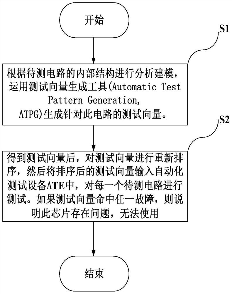
[0056] For integrated circuit testing, the main process is as follows:

[0057] S1. Perform analysis and modeling according to the internal structure of the circuit to be tested, and use a test vector generation tool (Automatic Test Pattern Generation, ATPG) to generate a test vector for the circuit. In this process, try to ensure that the circuit achieves a higher fault coverage rate.

[0058] S2. After the test vector is obtained, refer to the structure diagram of the tested integrated circuit to calculate the total critical area of ​​transistors in different unit circuits relative to the area coverage of the unit circuit. During the test process, each test vector hits the corresponding unit according to the statistics The number of circuit failures is estimated, the test characteristic value of each test vector is estimated, the original test set is reordered, and the sorted test vector set is input into the automated test equipment ATE to test each circuit to be tested. I...

Embodiment 2

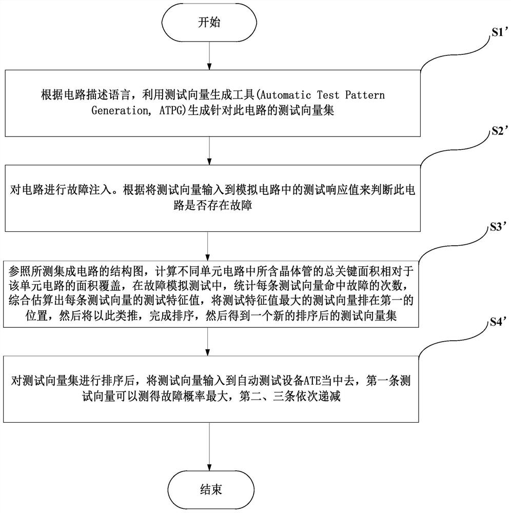
[0064] S1', according to the circuit description language, use a test vector generation tool (Automatic Test Pattern Generation, ATPG) to generate a test vector set for the circuit.

[0065] S2', perform fault injection on the circuit. According to the test response value inputting the test vector into the analog circuit, it is judged whether the circuit has a fault.

[0066] S3', referring to the structure diagram of the tested integrated circuit, calculate the total critical area of ​​the transistors contained in different unit circuits relative to the area coverage of the unit circuit, and in the fault simulation test, count the number of times that each test vector hits the fault, and comprehensively The test eigenvalues ​​of each test vector are estimated, and the test vector with the largest test eigenvalue is ranked first, and then by analogy, the sorting is completed, and a new sorted test vector set is obtained.

[0067] S4'. After sorting the test vector set, input ...


PUM


Abstract

The invention provides an effective key area parameter vector set reordering method and system. The method comprises the steps that a circuit description language of a tested integrated circuit is obtained, and a test vector set for the tested integrated circuit is generated by utilizing a test vector generation tool ATPG according to the circuit description language; performing fault injection on an analog circuit of the tested integrated circuit, and obtaining a test response value in the current analog circuit and judging whether the tested integrated circuit has a fault or not according to the test response value; processing the coverage of the total key area of transistors contained in different unit circuits relative to the area of the unit circuit by referring to the structure diagram of the tested integrated circuit, counting the number of times of hitting a fault by each test vector in the test vector set, and processing to obtain a test characteristic value according to the number of times of hitting the fault; and sorting and processing the test vectors according to the test characteristic values so as to resort a test vector set for testing the tested integrated circuit. According to the invention, the technical problems of high test cost, low test efficiency and low test accuracy of the integrated circuit are solved.

Description

technical field [0001] The present invention relates to an integrated circuit testing technology, in particular to a method and system for reordering an effective critical area parameter vector set. Background technique [0002] With the rapid development of the technology of the modern semiconductor industry, even chips composed of hundreds of millions of MOS tubes have come out. At the 2019 IEEE International Electronic Devices Conference (IEMD), chip giant Intel predicted that the chip manufacturing process node technology will maintain a 2-year leap. Controlling these properties becomes especially difficult with large circuit designs and shrinking feature sizes, resulting in increased diversity of manufacturing defects and reduced yields. As of the end of 2020, the total chip performance change rate has increased to 69%, which directly leads to a sharp increase in the number of test vectors under test, a significant increase in test time for automatic test equipment (AT...

Claims


Application Information

Patent Timeline
Patent Type & Authority Applications(China)
IPC IPC(8): G01R31/3181G01R31/3183G01R31/28
CPCG01R31/3181G01R31/3183G01R31/318307G01R31/318357G01R31/318364G01R31/2836
Inventor 詹文法张鲁萍江健生蔡雪原郑江云章礼华冯学军余储贤胡心怡
Owner ANQING NORMAL UNIV
Why Eureka
Try Eureka