
Plasma processing device

A plasma and processing device technology, applied in the field of plasma processing devices, can solve problems such as plasma difficulties and increase the volume of the reaction gas flow path 115, and achieve the effect of preventing deformation or damage

Inactive Publication Date: 2004-09-08
SHARP KK +1
View PDF0 Cites 1 Cited by
  • Summary
  • Abstract
  • Description
  • Claims
  • Application Information

AI Technical Summary

Problems solved by technology

However, if the height of the reaction gas channel 115 is increased in this way, the Figure 9 In the shown plasma processing apparatus, abnormal plasma is easily generated inside the reaction gas channel 115 by the microwave emitted from the shower plate 105.
Therefore, it is difficult to sufficiently increase the volume of the reaction gas flow path 115, and it is difficult to further improve the uniformity of the reaction gas supplied to the container interior 119 and further improve the uniformity of the plasma processing.

Method used


Image

  • Plasma processing device
  • Plasma processing device
  • Plasma processing device

Examples


Embodiment 1

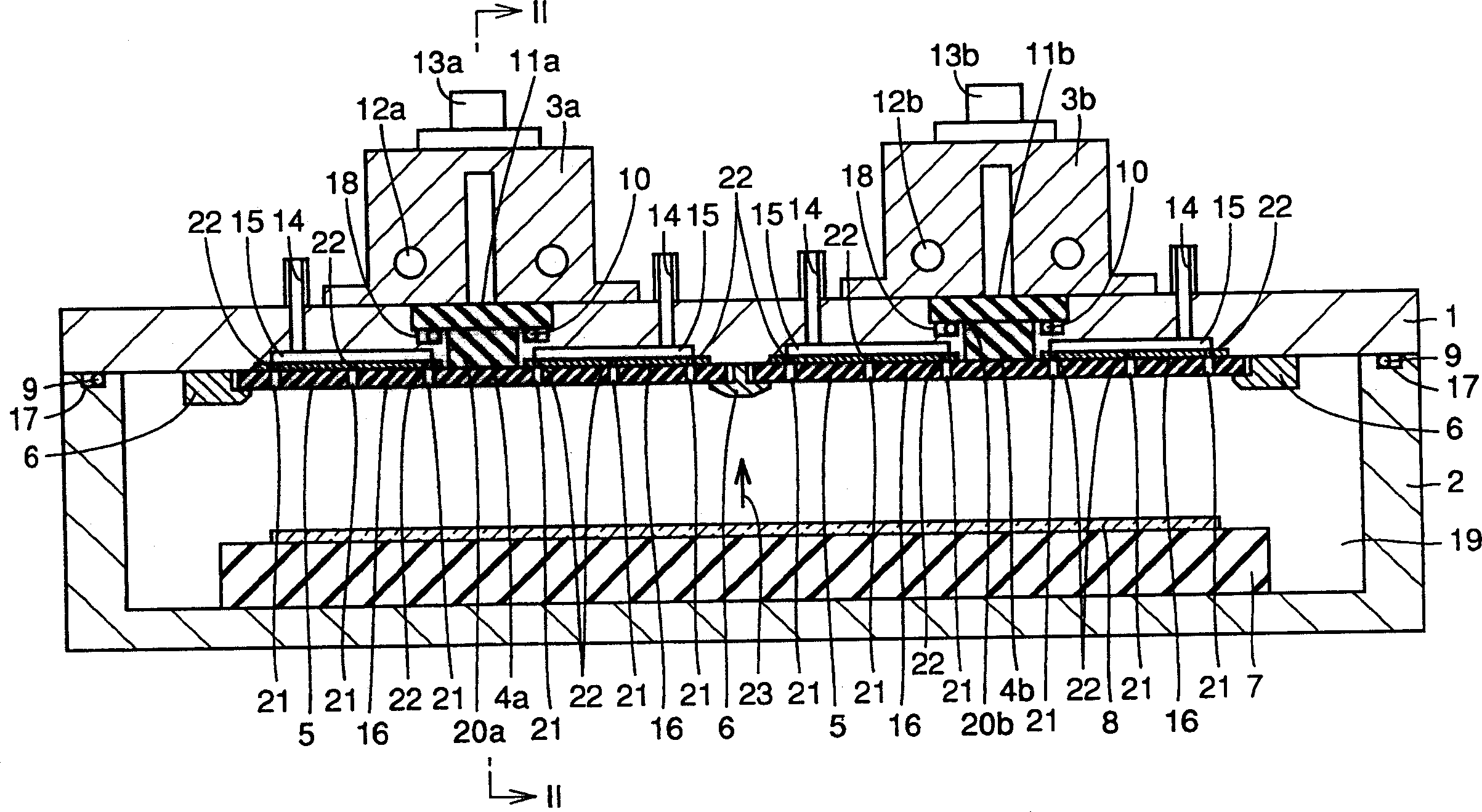
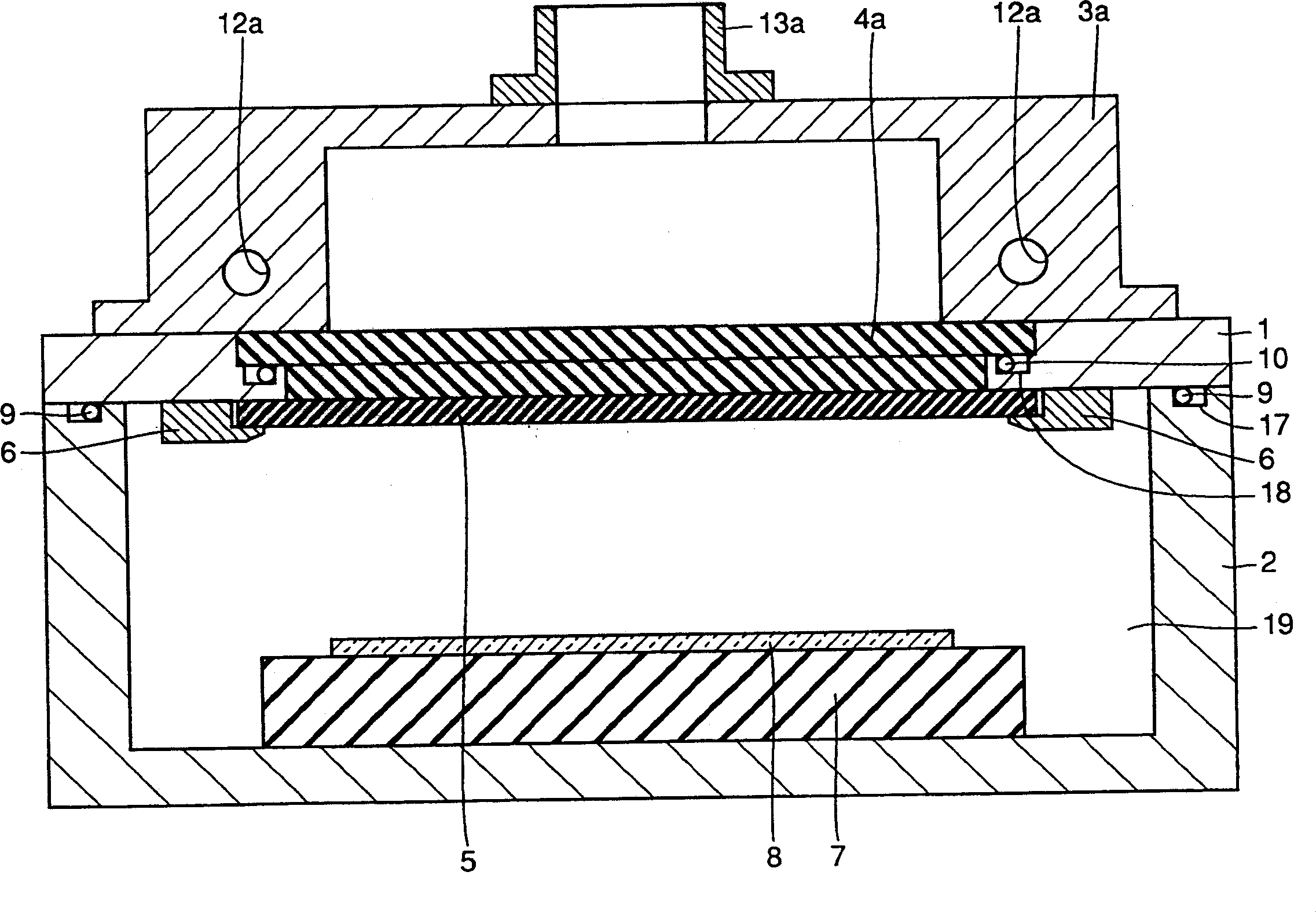
[0045] refer to figure 1 and figure 2 , Embodiment 1 of the plasma processing apparatus of the present invention will be described.

[0046] refer to figure 1 and figure 2 , The plasma processing apparatus includes: a container body 2; a container cover 1; a shower plate 5 as a microwave emitting member; microwave introduction windows 4a, 4b; waveguide ends 3a, 3b; The container lid 1 as a wall member is disposed on the upper opening of the container body 2 . A container as a processing chamber is composed of a container cover 1 and a container body 2 . On the connecting portion of the container cap 1 and the container body 2 , an O-ring groove 17 is formed on the container body 2 . The O-ring 9 is disposed inside the O-ring groove 17 . The connection portion between the container lid 1 and the container body 2 is sealed by an O-ring 9 . A substrate holder 7 is provided inside the container 19, and the holder 7 holds a substrate 8 to be subjected to plasma processing...

Embodiment 2

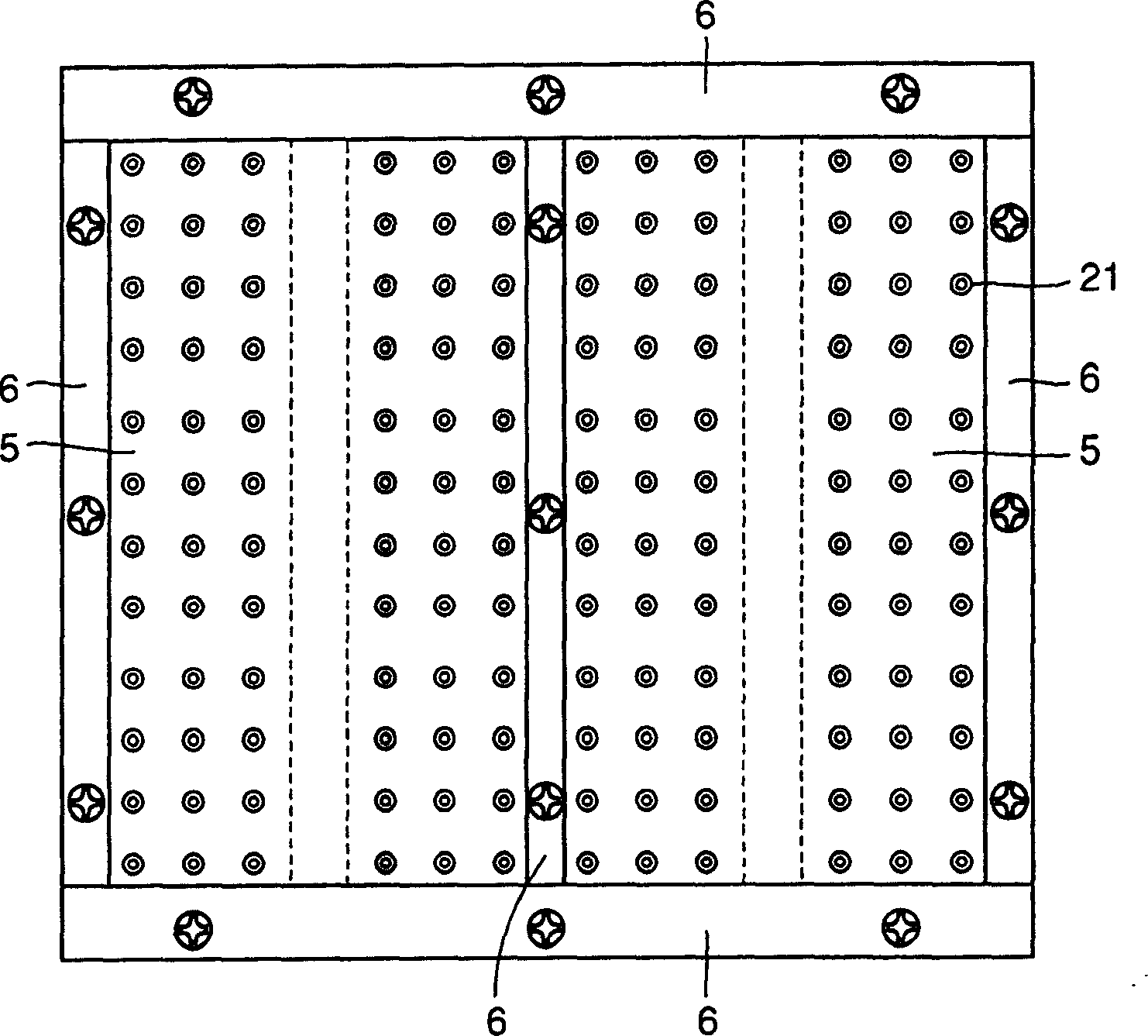
[0070] refer to figure 1 and image 3 In Embodiment 2 of the plasma processing apparatus of the present invention, the diameter of the gas introduction hole 21 of the shower plate 5 made of a dielectric such as alumina or aluminum nitride is made to be, for example, 1.0 mm. The diameter of the connection hole 22 of the metal plate 16 is changed in order to change the flow rate and the like of the reaction gas supplied to the container interior 19 . Specifically, a plurality of metal plates 16 having different diameters are prepared. Since processing of such a metal plate 16 is easier than processing of the shower plate 5, the plasma processing apparatus of this invention can be obtained more easily.

[0071] like image 3 and Figure 4 As shown, the diameter of the connection hole 22 is set to be smaller than the diameter of the gas introduction hole 21 . In this case, the diameter of the connection hole 22 can be made a dominant factor for changing the flow rate of the ...

Embodiment 3

[0073] Embodiment 3 of the plasma processing apparatus of the present invention has the same Figure 1-Figure 6 The plasma processing apparatus according to Example 1 of the present invention shown has the same structure, and the metal plate 16 and the container lid 1 are formed of the same material. By doing so, the thermal expansion ratios of the metal plate 16 and the container lid 1 can basically be equalized. Therefore, when the temperatures of the metal plate 16 and the container lid 1 increase with the plasma treatment, deformation or damage to the metal plate 16 due to the difference in thermal expansion between the metal plate 16 and the container lid 1 can be prevented. Furthermore, in consideration of the possibility that the metal plate 16 made of the same material as the container lid 1 may react with the supplied reaction gas, surface treatment such as anodizing treatment is required on the surface of the metal plate.


PUM


Abstract

The invention provides a plasma process apparatus capable of preventing generation of plasma in an unwanted location and performing uniform plasma processing with stability is obtained. The plasma process apparatus includes a processing chamber; a microwave radiating member and a reactive gas supply member, including a reactive gas supply passage having a space formed between the other wall surface of the microwave radiating member and the internal wall surface; and a microwave transmission preventing member disposed on a region, which faces the reactive gas supply passage, of the other wall surface of the microwave radiating member.

Description

technical field [0001] The present invention relates to a plasma processing apparatus, and more particularly, to a plasma processing apparatus capable of performing uniform plasma processing. Background technique [0002] Conventionally, in the manufacturing process of a liquid crystal display device, a semiconductor device, etc., a plasma processing apparatus using plasma is used in a film forming process, an etching process, an ashing process, and the like. In such a plasma processing apparatus, it is necessary to generate uniform plasma over the entire surface of the substrate to be processed in order to perform processing such as film formation uniformly on the entire surface to be processed of the substrate to be processed. [0003] In recent years, in the fields of semiconductor devices represented by semiconductor memory devices, liquid crystals, and the like, the size of substrates has been increased. In particular, in the case of a TFT (Thin Film Transistor) liquid...

Claims


Application Information

Patent Timeline
IPC IPC(8): H05H1/46B01J19/08C23C16/44C23C16/511H01J37/32H01L21/20H01L21/205H01L21/302H01L21/3065
CPCH01J37/32192C23C16/511C23C16/4401H01L21/20
Inventor 钟筑律夫田寺孝光山本达志平山昌树大见忠弘
Owner SHARP KK
Learn More