
Eureka
For R&D, Eureka makes reading and utilizing patents & technical documents easy.
Eureka AIR
Designed for self-driven R&D workflows. Generate viable solutions, solve complex R&D challenges, empower your innovation with AI.

Eureka Materials
Designed for material experts only. Revolutionize your material R&D, from search, analyze, to developing new materials.

TechResearch
Generate reliable direction feasibility study reports for your R&D in just a few steps.

TechSeek
Discover and master advanced knowledge NOW. Basics, ideas, possibilities, all at once.

TechMind
As an expert in R&D Theories, TechMind can generates customized viable solutions instantly.

TechRisk
Analyze your overall solution with one click, know your potential R&D risks in advance.

TechMonitor
Get weekly tech updates, stay abreast of the latest tech innovations and key insights.
Method for generating electrical conducting or semiconducting structures in two or three dimensions, method for erasing same structures and electric field generator/modulator
An electric field generator, semi-conductive technology, applied in semiconductor/solid-state device manufacturing, semiconductor devices, semiconductor/solid-state device components, etc., can solve complex problems
- Summary
- Abstract
- Description
- Claims
- Application Information
AI Technical Summary
Problems solved by technology
Method used
Image

Examples
example 1
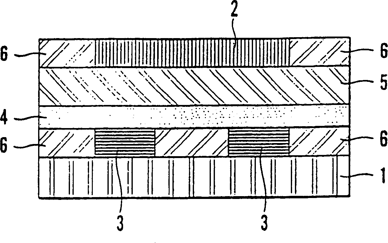
[0062] Figure 6 It shows that the forward-biased pn junction diode with conductive or semiconductive or conductive and semiconductive structure produced according to the method of the present invention is composed of four sublayers SS1-SS4 by thin film technology. Layers SS2 and SS3 contain active semiconducting material sandwiched between electrodes 11 in sublayers SS1 and SS4, respectively. The semiconductor material 10 in the sublayer SS2 is an n-type doped semiconductor, while the adjacent active material 10' in the sublayer SS3 is a p-type doped semiconductor. Electrodes 11 in sub-layers SS1 and SS4 are in contact with lateral conductive structures or conductive channels 9 in the same layer. Figure 6 The thickness of a single layer of the diode structure is typically 100 nm, and the thickness of the entire multilayer structure thus formed is less than 1 micron. The lateral extent of the diode structure area depends on the use with eg Figure 2a The spatial resolution ...
example 2-M
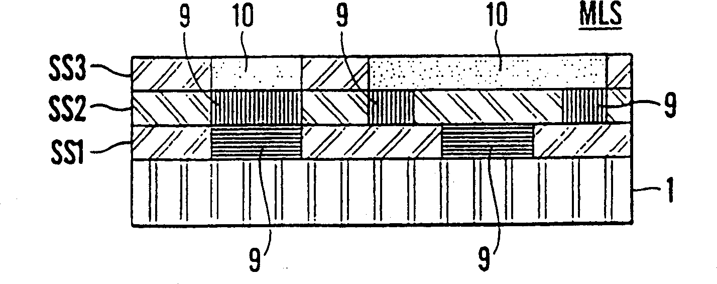
[0063] Example 2 - MOSFET
[0064] Figure 7 It schematically shows a MOSFET used in the present invention, which is made entirely of organic materials by thin film technology. The gate electrode 12 provided in the sublayer SS1 is connected to the lateral conductive structure 9 , while the sublayer SS2 constitutes the gate insulating layer 13 . Sub-layer SS3 provides semiconducting active material 10 and is aligned with gate electrode 10 . Source and drain electrodes 14 are provided by the uppermost layer SS4 and are connected to lateral conductive structures 9 in the same layer. Each sublayer consists of either a conductive structure or a semiconductive structure or a conductive structure and a semiconductive structure and a dielectric region. The thickness of this MOSFET can be 1 / 2 μm, and the range that can be realized by the current technology in the plane is from at most several microns to less than 1 μm, as described in Example 1.
example 3
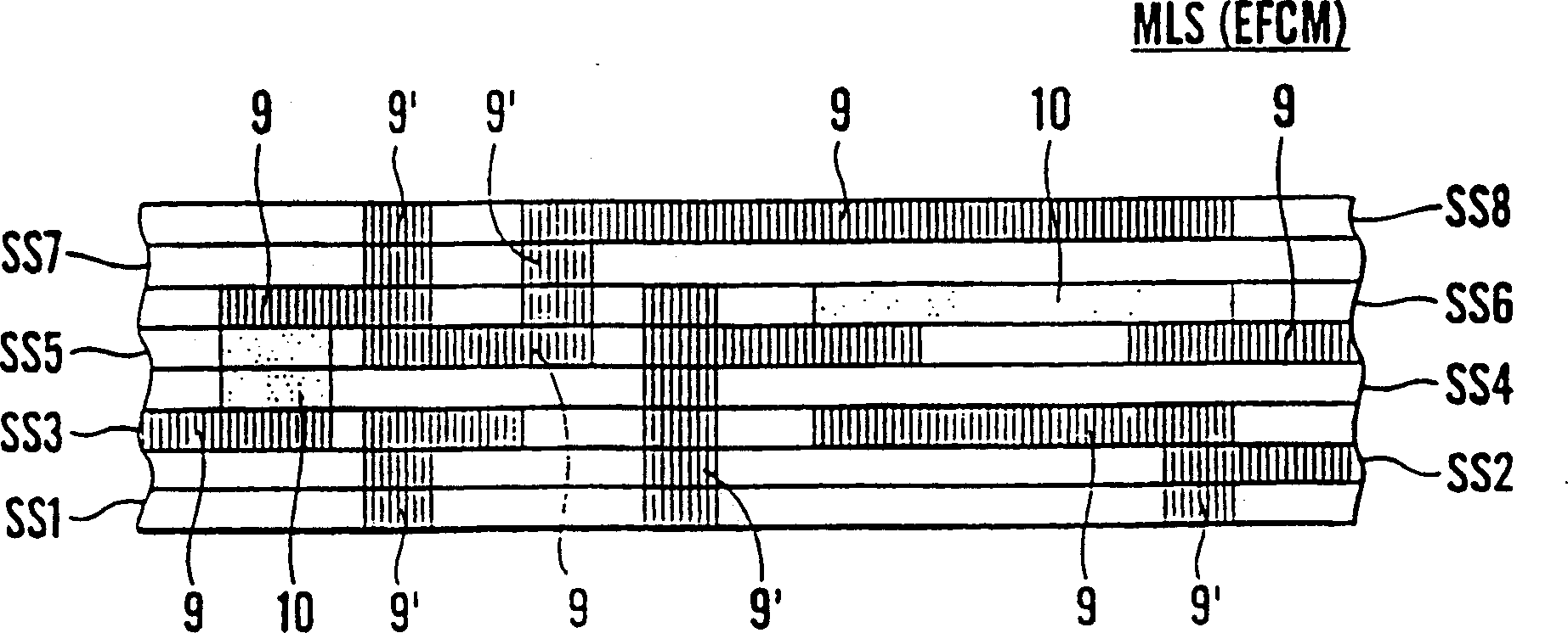
[0065] Example 3 - CMOS Logic Inverter
[0066] Figure 7 The MOSFET structure can now be used in logic gate circuits such as logic inverters in CMOS technology such as Figure 8 shown. This inverter is formed by connecting the source and drain electrodes of an n-MOSFET and a p-MOSFET in parallel in a back-to-back structure with a common gate electrode. For this purpose, a longitudinal conductive structure 15 is produced, which is connected to the electrode 14' through all the individual sublayers SS1-SS7. The output signal of the inverter is sent from the conductive structure 15 to the horizontal conductive structure 9 on the left in the figure. The common gate 12 of the MOSFET receives an input signal through the lateral conductive structure 9 in the right sublayer SS4 in the figure. The thickness of all sublayers is then less than 1 micron, and the typical thickness achieved is about 0.7 µm, while the lateral extent of the inverter will have the front combined Figur...
PUM
| Property | Measurement | Unit |
|---|---|---|
| thickness | aaaaa | aaaaa |
| thickness | aaaaa | aaaaa |
Abstract
Description
Claims
Application Information
 - R&D Engineer
- R&D Manager
- IP Professional
- Industry Leading Data Capabilities
- Powerful AI technology
- Patent DNA Extraction
Browse by: Latest US Patents, China's latest patents, Technical Efficacy Thesaurus, Application Domain, Technology Topic, Popular Technical Reports.
© 2024 PatSnap. All rights reserved.Legal|Privacy policy|Modern Slavery Act Transparency Statement|Sitemap|About US| Contact US: help@patsnap.com