Silicon solar cell of transparent conductive film front electrode

A transparent conductive film and solar cell technology, applied in semiconductor devices, circuits, photovoltaic power generation, etc., can solve problems such as inability to convert electricity, capture photogenerated carriers, and loss of solar cell conversion efficiency, so as to increase output power and improve Effect of short-wave spectral response and performance improvement

Inactive Publication Date: 2004-12-15
SICHUAN UNIV
View PDF0 Cites 0 Cited by
  • Summary
  • Abstract
  • Description
  • Claims
  • Application Information

AI Technical Summary

Problems solved by technology

It can absorb a lot of incident light (for example: 0.5μ silicon can absorb 9% of sunlight; 2μ thick sunlight is almost completely absorbed), but can not be converted into electricity
It also has a large number of structural defects, which will trap photo-generated carriers, making them unable to contribute to the photo-generated current
Therefore, a thick surface layer is also a non-negligible limitation for improving the conversion efficiency of solar cells.
[0011] Combining the above factors, a rough calculation shows that even if the existing crystalline silicon solar cells adopt an appropriate gate shallow density and matching surface thickness, the conversion efficiency of the solar cell will still be lost by about 30%.

Method used


Image

  • Silicon solar cell of transparent conductive film front electrode
  • Silicon solar cell of transparent conductive film front electrode
  • Silicon solar cell of transparent conductive film front electrode

Examples


Embodiment 1

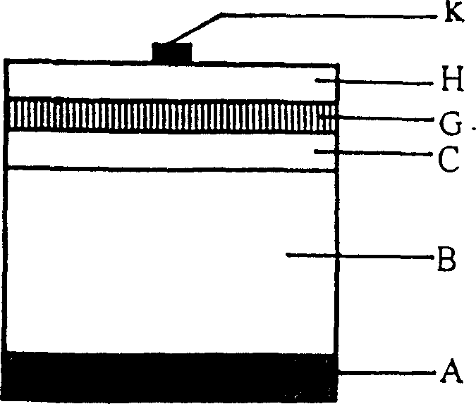
[0032] High-resistance transparent conductive film barrier layer using amorphous SnO 2 , Prepared by PECVD, high resistivity can be obtained. Generally resistivity ≥ 10 4 Ω.cm. The conductive layer of the high-conductivity transparent conductive film adopts doped SnO 2 . The specific implementation is as follows: first, a barrier layer (G) with a thickness of 5-10 nm is prepared by PECVD technology. Then prepare the conductive layer (H) of the high-conductivity transparent conductive film by the sputtering method, the low-pressure CVD method or the normal-pressure CVD method. The thickness is controlled to be 150-750 nm or thicker according to the anti-reflection conditions. Finally, the metal front electrode (K) is fabricated by screen printing, sputtering or vacuum evaporation. Generally, the density of front electrode strips is 0.5-2 strips / cm.

[0033] When amorphous SnO 2 The resistivity of the barrier layer is 10 4 Ω.cm, thickness 5nm; doped SnO 2 The conductivi...

Embodiment 2

[0035] High-resistance transparent conductive film barrier layer using amorphous SnO 2 , the conductive layer of high-conductivity transparent conductive film adopts ITO thin film, and can also use doped ZnO thin film or Cd 2 SnO 4 film. A barrier layer (G) of 5-10 nm is firstly prepared by PECVD technology. Then, the conductive layer (H) of the high-conductivity transparent conductive film is prepared by the sputtering method or the APCVD method, and the thickness is 150-750nm or thicker. Finally, the metal front electrode (K) was prepared as described in Example 1.

[0036] When amorphous SnO 2 The resistivity of the barrier layer is 10 4 Ω.cm, the thickness is 5nm; the conductivity of the conductive layer of the ITO transparent conductive film is 1.5×10 4 (Ω.cm) -1 , when the thickness is 600nm, the conversion efficiency is about 35% higher than that of the grid-shaped front electrode.

Embodiment 3

[0038] High resistance transparent conductive film barrier layer SnO 2 Polycrystalline film is used, and the conductive layer of high-conductivity transparent conductive film adopts doped SnO 2 thin film or ITO film, or doped ZnO thin film, Cd 2 SnO 4 film. Firstly, an undoped high-resistance transparent conductive film barrier layer (G) is prepared by low-pressure CVD or normal-pressure CVD. Since its resistivity is between 5-10Ω.cm, its thickness is controlled at about 100nm. Then, according to the technique described in Example 1 or Example 2, a conductive layer (H) of a high-conductivity transparent conductive film is produced, with a thickness of 150-750 nm, or thicker. That is, SnO can be prepared by sputtering method, low pressure CVD method or normal pressure CVD method 2 Polycrystalline thin film transparent conductive film conductive layer; or use sputtering method, normal pressure CVD method to prepare ITO film; or use other methods to prepare doped ZnO thin fi...


PUM

PropertyMeasurementUnit
electrical resistivityaaaaaaaaaa

Abstract

The transparent electric film is utilized as the front electrode to replace the fence type from electrode and the layer for reducing the reflection. The from electrode of the transparent electric film in the invention is laminated structure. That is prepared by following steps. The transparent electric film with high resistance and the thickness less than 100nm are prepared on the silicon substrate with the n-p node having been formed. Then, the transparent electric film with high conductance and the thickness larger than 150nm is prepared according to the requirement of the conductance and the reduced reflection. Comparing to the prior art, the invention makes the conversion efficiency increase 25-35%.

Description

1. Technical field [0001] The invention belongs to a photovoltaic cell with a new structure. 2. Background technology [0002] The basic structure of existing crystalline silicon (monocrystalline silicon, polycrystalline silicon) solar cells is as follows: figure 1 shown. It consists of a crystalline silicon (B) with a planar semiconductor n-p junction (C), plus a back electrode (A) and a front electrode (E). The front electrode is very critical. It can neither block the incident light to ensure that most of the incident light enters the n-p junction, but also fully collect the photogenerated carriers. These are two conflicting requirements. The current technology is to use a metal grid electrode to solve this contradiction. [0003] In order to reduce the reflection of sunlight on the silicon surface, an optical anti-reflection layer (F) is usually used. They are insulating films such as silicon monoxide (SiO) and silicon nitride (SiN) with a refractive index between 2...

Claims


Application Information

Patent Timeline
Patent Type & Authority Patents(China)
IPC IPC(8): H01L31/0224H01L31/06
CPCH01L31/02168Y02E10/50Y02E10/547
Inventor 冯良桓蔡亚平
Owner SICHUAN UNIV
Why Eureka
Try Eureka