Method for mfg. electronic elements and apparatus for mfg. film
A manufacturing method and technology for electronic components, which are applied in the directions of electrical components, spraying devices, spraying devices, etc., can solve the problems of reducing the reliability of electronic components, lowering the film-forming efficiency of the device, and reducing the
- Summary
- Abstract
- Description
- Claims
- Application Information
AI Technical Summary
Problems solved by technology
Method used
Image
Examples
Embodiment 1
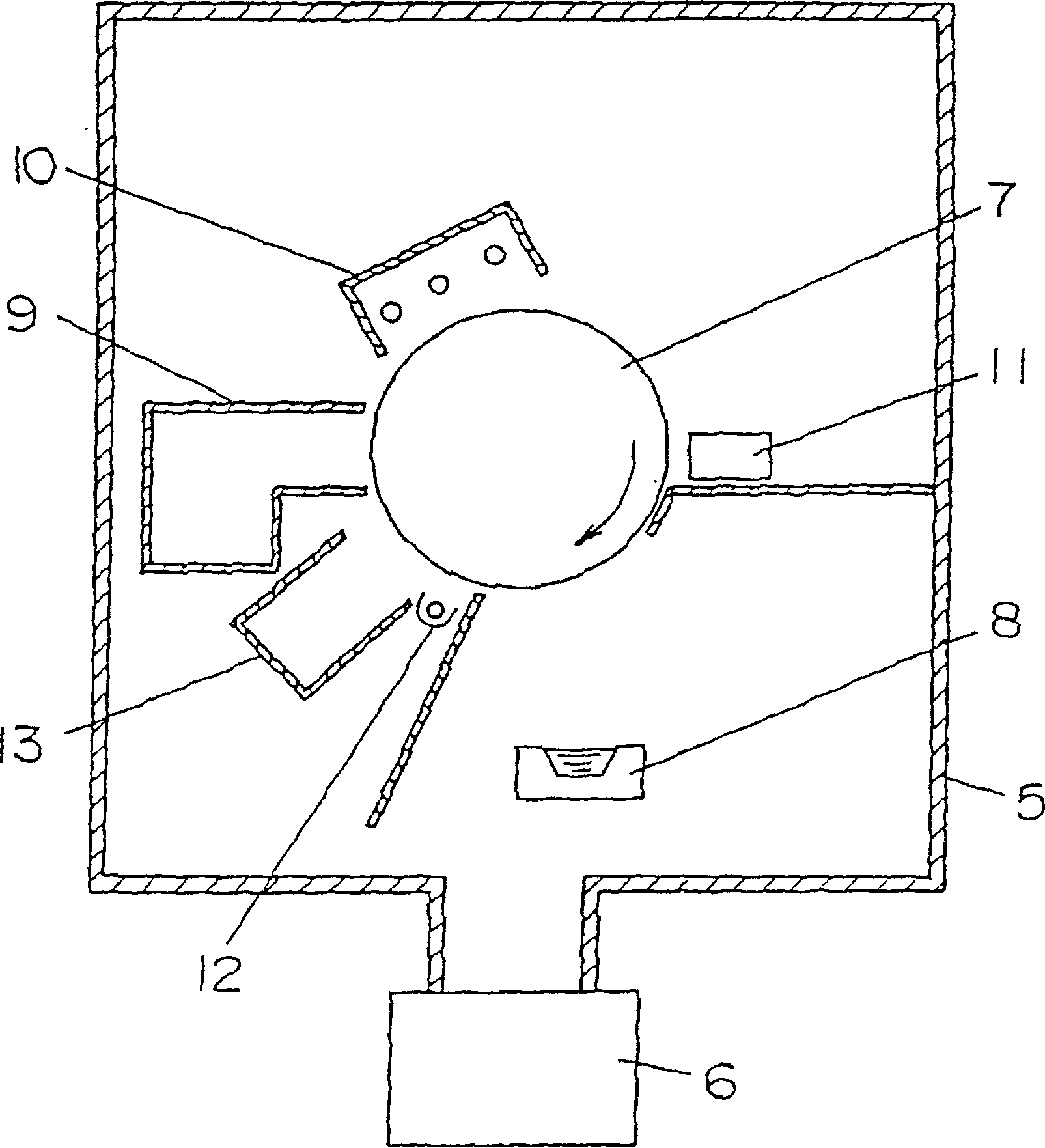
[0047] use figure 1 The apparatus shown produces laminates for capacitors.
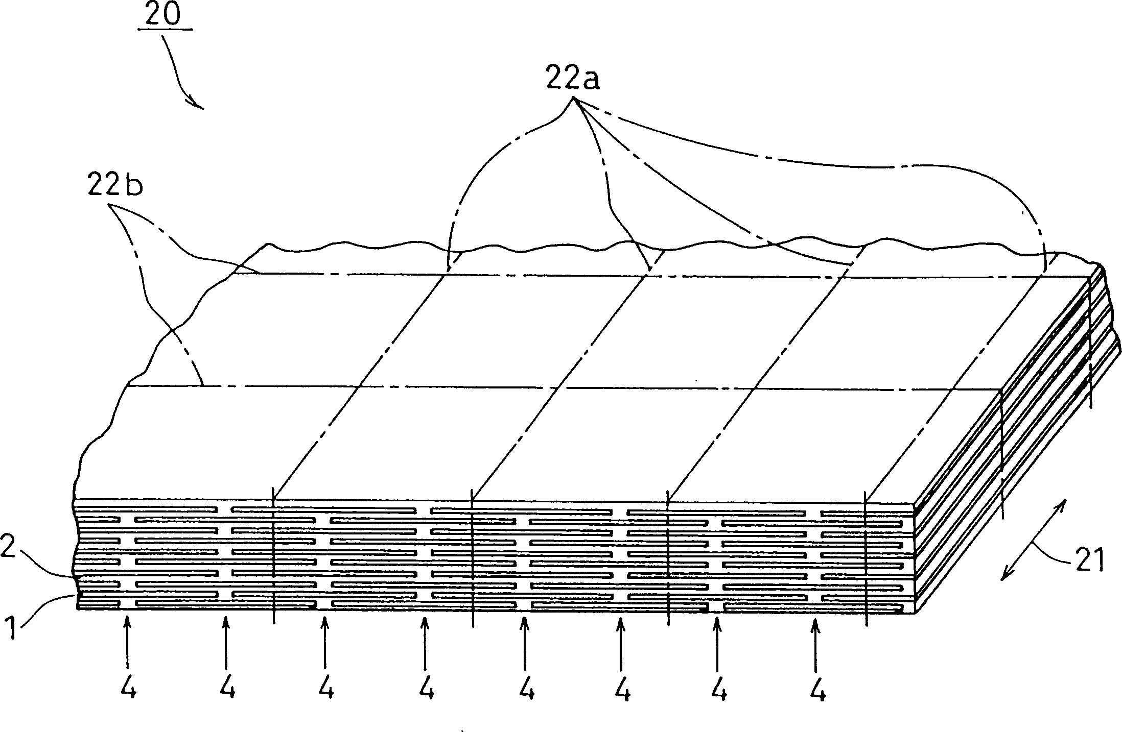
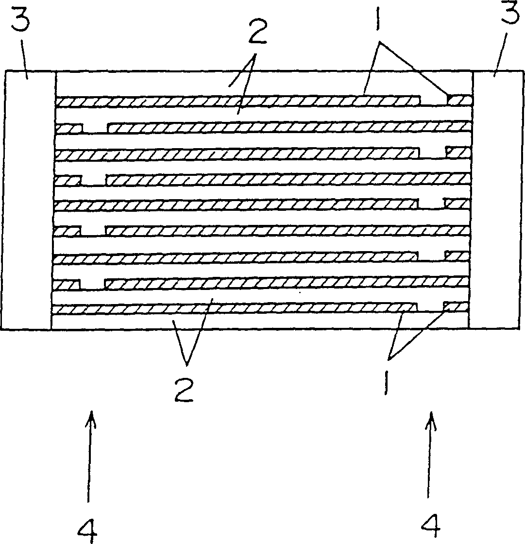
[0048] An evaporated film of aluminum as a metal film and an acrylic resin film produced by vaporization by electric heating as a dielectric film are formed on the roll 7 . At this time, the resin film is irradiated with ultraviolet rays to harden it, and the metal film is patterned into a predetermined shape by oil-limited patterning. After stacking to a predetermined number of layers, the laminate is separated from the drum 7 to obtain the following: figure 2 The laminated base element 20 shown is subjected to post-processing such as cutting and forming of external electrodes, to form a capacitor. image 3 A schematic diagram showing the cross-sectional structure pattern of the manufactured capacitor.
[0049] The aluminum thin film had a thickness of 50 nm, and the resin thin film had a thickness of 1 μm. As the resin material, a mixture of 1.9 nonanediol diacrylate and 5 wt % photoreinitiato...
Embodiment 2
[0056] use figure 1 The apparatus shown produces laminates for capacitors.
[0057] An evaporated film of aluminum as a metal film and an acrylic resin film produced by gasification by electric heating as a dielectric film are formed on the roller 7 . At this time, the resin film is irradiated with ultraviolet rays to harden it, and the metal film is patterned in a predetermined shape by an oil patterning method. After stacking to a predetermined number of stacks, the laminate is separated from the drum 7 to obtain figure 2 The multilayer parent element shown in the figure is further processed by cutting, forming external electrodes, etc., to obtain a capacitor. image 3 A schematic diagram showing a schematic cross-sectional structure of a manufactured capacitor.
[0058] The aluminum thin film had a thickness of 50 nm, and the resin thin film had a thickness of 1 μm. As the resin material, a mixture of 1.9 nonanediol diacrylate and 5 wt % photoreinitiator was used. Th...
Embodiment 3
[0060] use figure 1 The apparatus shown produces laminates for capacitors.
[0061] An evaporated copper film as a metal film and an acrylic resin film produced by vaporization by electric heating as a dielectric film are formed on the roll 7 . At this time, the resin film is irradiated with ultraviolet rays to harden it, and the metal film is patterned into a predetermined shape by oil-limited patterning. After stacking to a predetermined number of layers, the laminate is separated from the drum 7 to obtain the following: figure 2 The laminated base element 20 shown is subjected to post-processing such as cutting and forming of external electrodes, to form a capacitor. image 3 A schematic diagram showing the cross-sectional structure pattern of the manufactured capacitor.
[0062]The copper thin film had a thickness of 40 nm, and the resin thin film had a thickness of 0.1 μm. As the resin material, dimethanol tricyclodecane diacrylate was used. Copper thin film and re...
PUM
| Property | Measurement | Unit |
|---|---|---|
| thickness | aaaaa | aaaaa |
Abstract
Description
Claims
Application Information


