
Low vacuum bonding method of polydimethylsiloxane chip

A technology of polydimethylsiloxane and low vacuum, which is applied in the direction of material inspection products, instruments, and analytical materials. It can solve the problems of high chip temperature rise, chip performance impact, and difficulty in laboratory implementation, and achieve simple equipment. Effect

Inactive Publication Date: 2005-04-06
XIAMEN UNIV
View PDF0 Cites 0 Cited by
  • Summary
  • Abstract
  • Description
  • Claims
  • Application Information

AI Technical Summary

Problems solved by technology

Therefore, the overall requirements for equipment are relatively high, and it is difficult for general laboratories to achieve
In addition, the general oxygen plasma treatment time is 40-60s, which makes the chip temperature rise higher, easily destroys the surface chemical composition of the chip, and affects the performance of some chips

Method used


Image

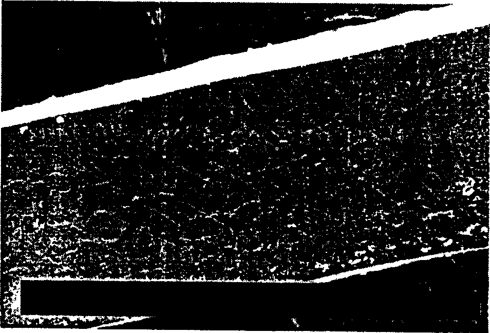
  • Low vacuum bonding method of polydimethylsiloxane chip
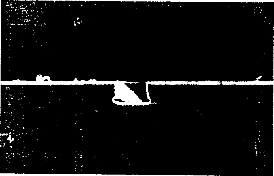
  • Low vacuum bonding method of polydimethylsiloxane chip
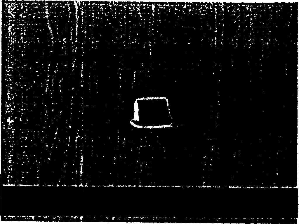
  • Low vacuum bonding method of polydimethylsiloxane chip

Examples


Embodiment 1

[0027] Pour the silicone rubber material into the chip mold, and peel it off freshly after polymerization to obtain the PDMS chip assembly, put it into the vacuum chamber, and evacuate until the background vacuum of the chamber is 26.6Pa; rinse with oxygen repeatedly 3 times, discharge the residual gas, Turn off the oxygen flow, then evacuate (that is, the oxygen pressure) to 39.9Pa, and apply a high voltage of 1400V (current is 220mA) to make the oxygen in the chamber glow and bombard the surface of the PDMS chip with oxygen plasma for 40s; open the vent valve , Inflate the vacuum chamber to the equilibrium with the atmospheric pressure, then open the vacuum chamber, attach the chips, and keep warm at 100°C for 2 hours to achieve irreversible bonding.

[0028] After oxygen plasma treatment, the surface of the PDMS chip has a strong hydrophilicity, and its contact angle is close to 0°, but the hydrophilicity gradually deteriorates with time, and it almost returns to the untreat...

Embodiment 2

[0033]Pour the silicone rubber material into the chip mold, and freshly peel off after polymerization to obtain the PDMS chip component, put it into the vacuum chamber, and evacuate it until the background vacuum of the chamber is 19.95Pa; wash it twice with oxygen repeatedly, and discharge the residual gas. Turn off the oxygen flow, then evacuate (that is, the oxygen pressure) to 33.25Pa, and apply a high voltage of 2000V (current is 380mA), so that the oxygen in the cavity is glowed, and the oxygen plasma is bombarded on the surface of the PDMS chip for 5s; open the vent valve , Inflate the vacuum chamber to the equilibrium with the atmospheric pressure, then open the vacuum chamber, attach the chips, and keep warm at 120°C for 1.5h to achieve irreversible bonding.

[0034] After oxygen plasma treatment, the surface of the PDMS chip has a strong hydrophilicity, and its contact angle is close to 0°, but the hydrophilicity gradually deteriorates with time, and it almost returns...

Embodiment 3~10

[0036] Example

[0037] Experiments have shown that the hydrophilicity of PDMS chips treated with oxygen plasma has been greatly improved, and water droplets can spread rapidly on the PDMS surface (the contact angle is close to 0°).


PUM


Abstract

The invention refers to a low-vacuum bonding method for a polydimethylsiloxane chip, its steps: freshly peel off the polymerized silicon latex sample to obtain chip subassembly, place in vacuum cavity, vacuumize, wash by oxygen again and again, and eliminate the remnant gas; vacuumize again, exert high pressure to make the oxygen light up in the vacuum cavity, to make oxygen plasm bombardment on the chip subassembly's surface, the air pressure equal to the atmospheric pressure, open the vacuum cavity, and joint the chip subassembly. It has very high bonding intensity, able to surpass that of PDMS noumenon.

Description

(1) Technical field [0001] The invention relates to a low-vacuum bonding method, in particular to a low-vacuum bonding method for polydimethylsiloxane chips. (2) Background technology [0002] Microfluidic chip (microfluidic chip) has a broad application prospect in the fields of analysis system, biomedicine, chemistry and biochemistry. The traditional microfluidic chip follows the IC industrial technology, and mainly uses silicon and glass as materials; therefore, it must go through a series of processes such as mask making, photolithography, and microchannel etching. The manufacturing process is complex, the cycle is long, and the efficiency is high. It is relatively low, and the sidewalls of microfluidic channels etched on such hard materials are difficult to be both smooth and steep. However, using high molecular polymers as materials to make microfluidic chips can overcome the above difficulties, thereby realizing low-cost, high-volume, and high-efficiency manufacturin...

Claims


Application Information

Patent Timeline
Patent Type & Authority Patents(China)
IPC IPC(8): C12Q1/68G01N27/26G01N27/416G01N33/68G01N35/00
Inventor 沈德新周勇亮罗仲梓
Owner XIAMEN UNIV
Learn More